Recap from Part 1
In Part 1 of this post series, we discussed ECAM and how configuration space accesses looked in both software and on the hardware packet network. In that discussion, the concepts of TLPs (Transaction Layer Packets) were introduced, which is the universal packet structure by which all PCIe data is moved across the hierarchy. We also discussed how these packets move similar to Ethernet networks in that an address (the BDF in this case) was used by routing devices to send Configuration Space packets across the network.
Configuration space reads and writes are just one of the few ways that I/O can be performed directly with a device. Given its “configuration” name, it is clear that its intention is not for performing large amounts of data transfer. The major downfall is its speed, as a configuration space packet can only contain at most 64-bits of data being read or written in either direction (often only 32-bits). With that tiny amount of usable data, the overhead of the packet and other link headers is significant and therefore bandwidth is wasted.
As discussed in Part 1, understanding memory and addresses will continue to be the key to understanding PCIe. In this post, we will look more in-depth into the much faster forms of device I/O transactions and begin to form an understanding of how software device drivers actually interface with PCIe devices to do useful work. I hope you enjoy!
NOTE: You do not need to be an expert in computer architecture or TCP/IP networking to get something from this post. However, knowing the basics of TCP/IP and virtual memory is necessary to grasp some of the core concepts of this post. This post also builds off of information from Part 1. If you need to review these, do so now!
Introduction to Data Transfer Methods in PCIe
Configuration space was a simple and effective way of communicating with a device by its BDF during enumeration time. It is a simple mode of transfer for a reason - it must be the basis by which all other data transfer methods are configured and made usable. Once the device is enumerated, configuration space has set up all of the information the device needs to perform actual work together with the host machine. Configuration space is still used to allow the host machine to monitor and respond to changes in the state of the device and its link, but it will not be used to perform actual high speed transfer or functionality of the device.
What we now need are data transfer methods that let us really begin to take advantage of the high-speed transfer throughput that PCIe was designed for. Throughput is a measurement of the # of bytes transferred over a given period of time. This means to maximize throughput, we must minimize the overhead of each packet to transfer the maximum number of bytes per packet. If we only send a few DWORDs (4-bytes each) per packet, like in the case of configuration space, the exceptional high-speed transfer capabilities of the PCIe link are lost.
Without further ado, let’s introduce the two major forms of high-speed I/O in PCIe:
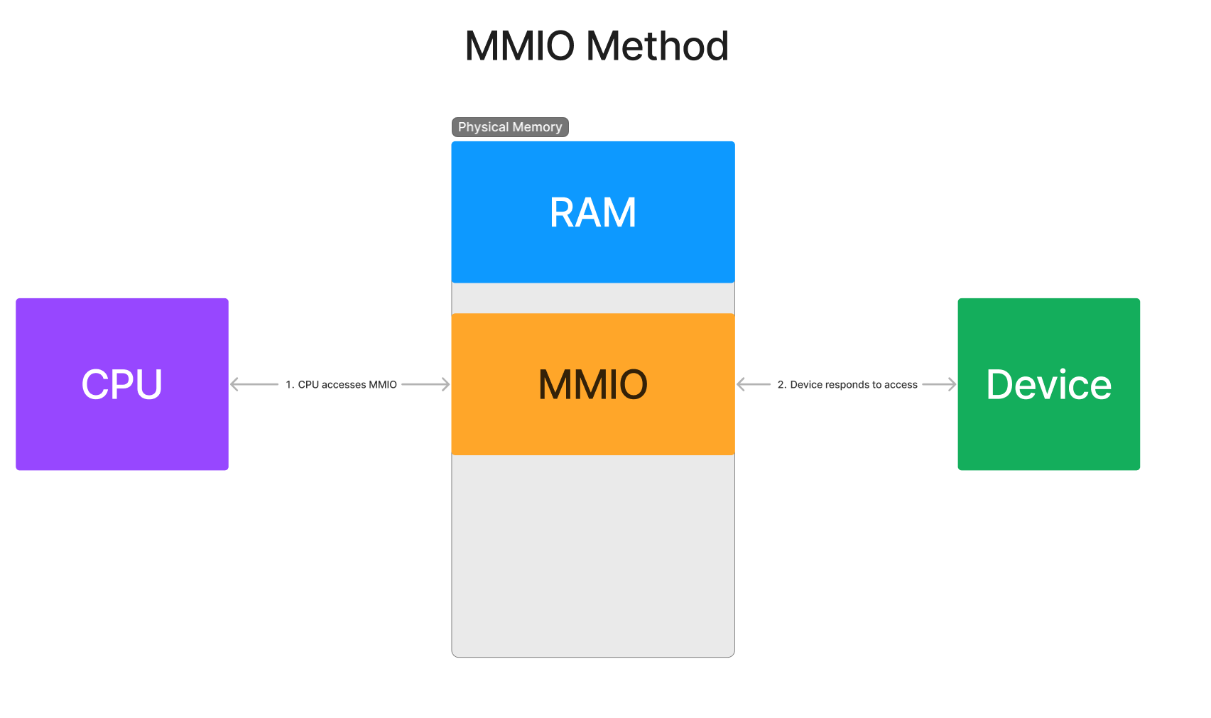
- Memory Mapped Input/Output (abbrev. MMIO) - In the same way the host CPU reads and writes memory to ECAM to perform config space access, MMIO can be used to map an address space of a device to perform memory transfers. The host machine configures “memory windows” in its physical address space that gives the CPU a window of memory addresses which magically translate into reads and writes directly to the device. The memory window is decoded inside the Root Complex to transform the reads and writes from the CPU into data TLPs that go to and from the device. Hardware optimizations allow this method to achieve a throughput that is quite a bit faster than config space accesses. However, its speed still pales in comparison to the bulk transfer speed of DMA.
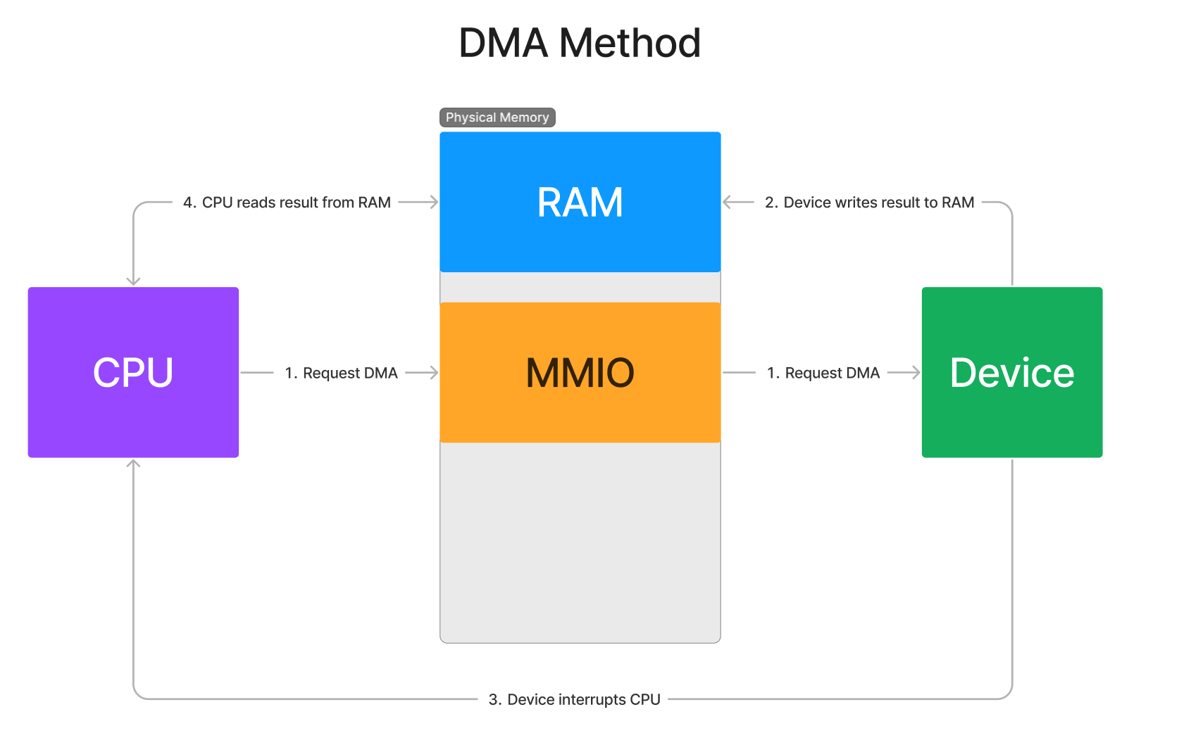
- Direct Memory Access (abbrev. DMA) - DMA is by far the most common form of data transfer due to its raw transfer speed and low latency. Whenever a driver needs to do a transfer of any significant size between the host and the device in either direction, it will assuredly be DMA. But unlike MMIO, DMA is initiated by the device itself, not the host CPU. The host CPU will tell the device over MMIO where the DMA should go and the device itself is responsible for starting and finishing the DMA transfer. This allows devices to perform DMA transactions without the CPU’s involvement, which saves a huge number of CPU cycles than if the device had to wait for the host CPU to tell it what to do each transfer. Due to its ubiquity and importance, it is incredibly valuable to understand DMA from both the hardware implementation and the software interface.
Introduction to MMIO
What is a BAR?
Because configuration space memory is limited to 4096 bytes, there’s not much useful space left afterwards to use for device-specific functionality. What if a device wanted to map a whole gigabyte of MMIO space for accessing its internal RAM? There’s no way that can fit that into 4096 bytes of configuration space. So instead, it will need to request what is known as a BAR (Base Address Register) . This is a register exposed through configuration space that allows the host machine to configure a region of its memory to map directly to the device. Software on the host machine then accesses BARs through memory read/write instructions directed to the BAR’s physical addresses, just as we’ve seen with the MMIO in ECAM in Part 1. Just as with ECAM, the act of reading or writing to this mapping of device memory will translate directly into a packet sent over the hierarchy to the device. When the device needs to respond, it will send a new packet back up through the hierarchy to the host machine.
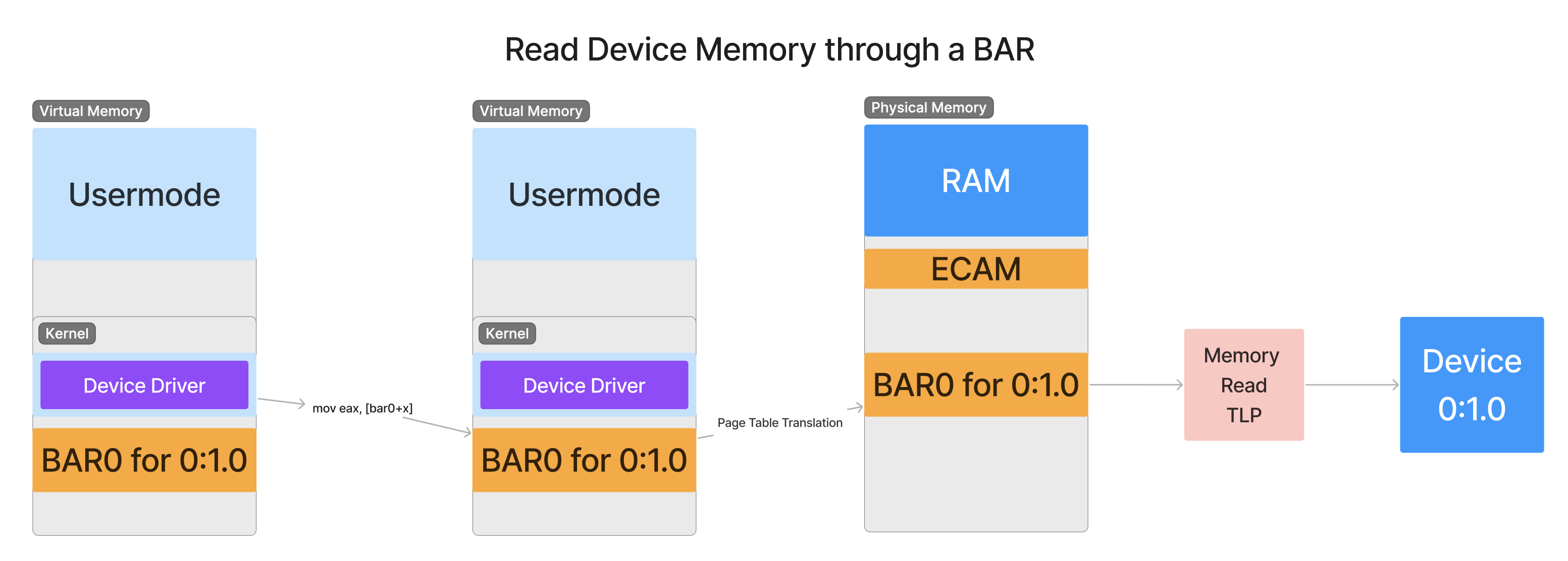
When a CPU instruction reads the memory of a device’s MMIO region, a Memory Read Request Transaction Layer Packet (MemRd TLP) is generated that is transferred from the Root Complex of the host machine down to the device. This type of TLP informs the receiver that the sender wishes to read a certain number of bytes from the receiver. The expectation of this packet is that the device will respond with the contents at the requested address as soon as possible.
All data transfer packets sent and received in PCIe will be in the form of these Transaction Layer Packets. Recall from Part 1 that these packets are the central abstraction by which all communication between devices takes place in PCIe. These packets are reliable in the case of data transfer errors (similar to TCP in networking) and can be retried/resent if necessary. This ensures that data transfers are protected from the harsh nature of electrical interference that takes place in the extremely high speeds that PCIe can achieve. We will look closer at the structure of a TLP soon, but for now just think of these as regular network packets you would see in TCP.
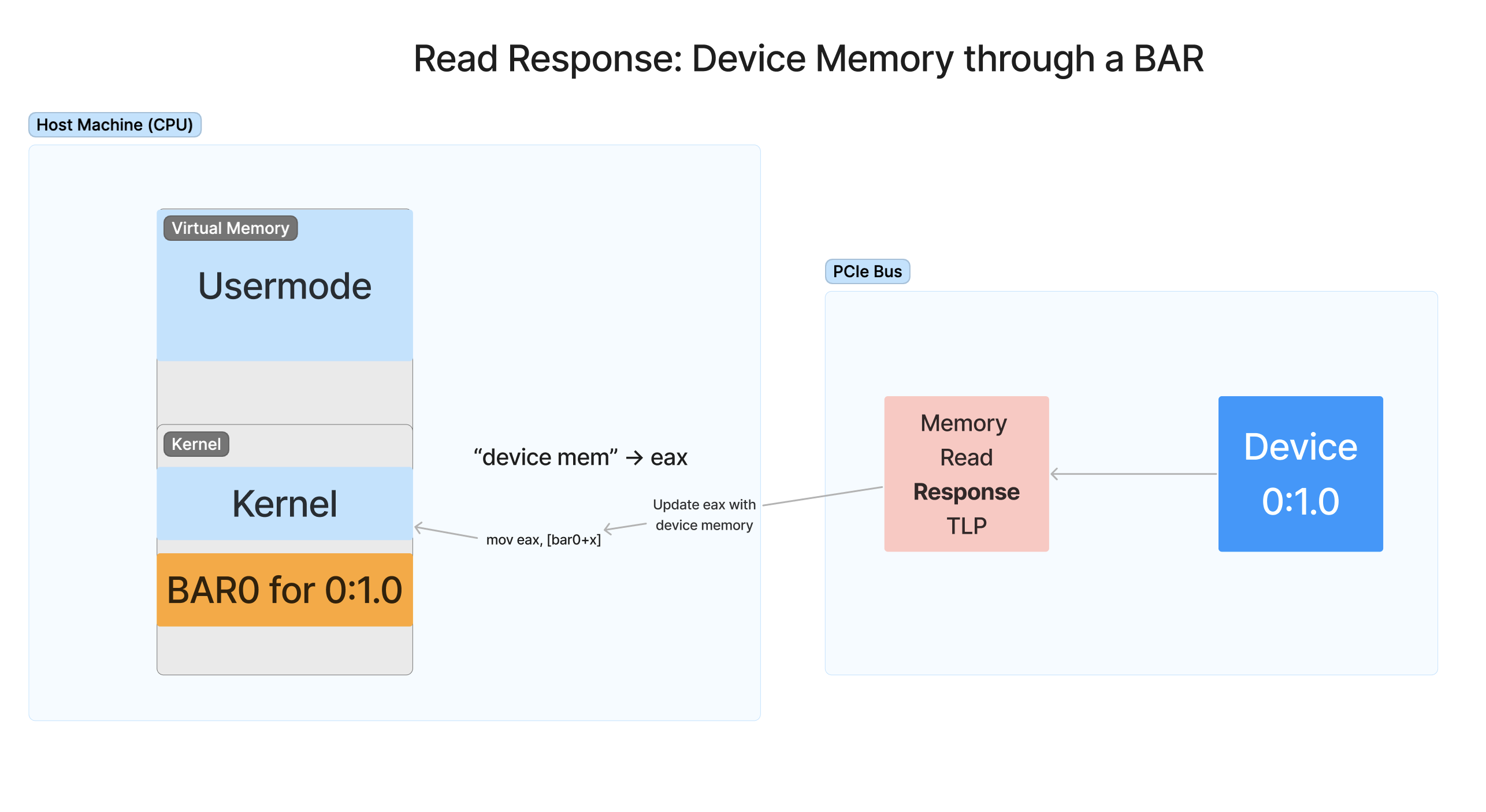
When the device receives the requestor packet, the device responds to the memory request with a Memory Read Response TLP. This TLP contains the result of the read from the device’s memory space given the address and size in the original requestor packet. The device marks the specific request packet and sender it is responding to into the response packet, and the switching hierarchy knows how to get the response packet back to the requestor. The requestor will then use the data inside the response packet to update the CPU’s register of the instruction that produced the original request.
In the meantime while a TLP is in transit, the CPU must wait until the memory request is complete and it cannot be interrupted or perform much useful work. As you might see, if lots of these requests need to be performed, the CPU will need to spend a lot of time just waiting for the device to respond to each request. While there are optimizations at the hardware level that make this process more streamlined, it still is not optimal to use CPU cycles to wait on data transfer to be complete. Hopefully you see that we need a second type of transfer, DMA, to address these shortcomings of BAR access.
Another important point here is that device memory does not strictly need to be for the device’s - RAM. While it is common to see devices with onboard RAM having a mapping of its internal RAM exposed through a BAR, this is not a requirement. For example, it’s possible that accessing the device’s BAR might access internal registers of the device or cause the device to take certain actions. For example, writing to a BAR is the primary way by which devices begin performing DMA. A core takeaway should be that device BARs are very flexible and can be used for both controlling the device or for performing data transfer to or from the device.
How BARs are Enumerated
Devices request memory regions from software using its configuration space. It is up to the host machine at enumeration time to determine where in physical memory that region is going to be placed. Each device has six 32-bit values in its configuration space (known as “registers”, hence the name Base Address Register) that the software will read and write to when the device is enumerated. These registers describe the length and alignment requirements of each of the MMIO regions the device wishes to allocate, one per possible BAR up to a total of six different regions. If the device wants the ability to map its BAR to above the 4GB space (a 64-bit BAR), it can combine two of the 32-bit registers together to form one 64-bit BAR, leaving a maximum of only three 64-bit BARs. This retains the layout of config space for legacy purposes.
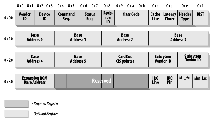
TERMINOLOGY NOTE: Despite the acronym BAR meaning Base Address Register, you will see the above text refers to the memory window of MMIO as a BAR as well. This unfortunately means that the name of the register in configuration space is also the same name as the MMIO region given to the device (both are called BARs). You might need to read into the context of what is being talked about to determine if they mean the window of memory, or the actual register in config space itself.
BARs are another example of a register in config space that is not constant. In Part 1, we looked at some constant registers such as VendorID and DeviceID. But BARs are not constant registers, they are meant to be written and read by the software. In fact, the values written to the registers by the software are special in that writing certain kinds of values to the register will result in different functionality when read back. If you haven’t burned into your brain the fact that device memory is not always RAM and one can read values back different than what was written, now’s the time to do that.
Device memory can be RAM, but it is not always RAM and does not need to act like RAM!
What is DMA? Introduction and Theory
We have seen two forms of I/O so far, the config space access and the MMIO access through a BAR. The last and final form of access we will talk about is Direct Memory Access (DMA). DMA is by far the fastest method of bulk transfer for PCIe because it has the least transfer overhead. That is, the least amount of resources are required to transfer the maximum number of bytes across the link. This makes DMA absolutely vital for truly taking advantage of the high speed link that PCIe provides.
But, with great power comes great confusion. To software developers, DMA is a very foreign concept because we don’t have anything like it to compare to in software. For MMIO, we can conceptualize the memory accesses as instructions reading and writing from device memory. But DMA is very different from this. This is because DMA is asynchronous, it does not utilize the CPU in order to perform the transfer. Instead, as the name implies, the memory read and written comes and goes directly from system RAM. The only parties involved once DMA begins is the memory controller of the system’s main memory and the device itself. Therefore, the CPU does not spend cycles waiting for individual memory access. It instead just initiates the transfer and lets the platform complete the DMA on its own in the background. The platform will then inform the CPU when the transfer is complete, typically through an interrupt.
Let’s think for a second why this is so important that the DMA is performed asynchronously. Consider the case where the CPU is decrypting a huge number of files from a NVMe SSD on the machine. Once the NVMe driver on the host initiates DMA, the device is constantly streaming file data as fast as possible from the SSD’s internal storage to locations in system RAM that the CPU can access. Then, the CPU can use 100% of its processing power to perform the decryption math operations necessary to decrypt the blocks of the files as it reads data from system memory. The CPU spends no time waiting for individual memory reads to the device, it instead just hooks up the firehose of data and allows the device to transfer as fast as it possibly can, and the CPU processes it as fast as it can. Any extra data is buffered in the meantime within the system RAM until the CPU can get to it. In this way, no part of any process is waiting on something else to take place. All of it is happening simultaneously and at the fastest speed possible.
Because of its complexity and number of parts involved, I will attempt to explain DMA in the most straightforward way that I can with lots of diagrams showing the process. To make things even more confusing, every device has a different DMA interface. There is no universal software interface for performing DMA, and only the designers of the device know how that device can be told to perform DMA. Some device classes thankfully use a universally agreed upon interface such as the NVMe interface used by most SSDs or the XHCI interface for USB 3.0. Without a standard interface, only the hardware designer knows how the device performs DMA, and therefore the company or person producing the device will need to be the one writing the device driver rather than relying on the universal driver bundled with the OS to communicate with the device.
A “Simple” DMA Transaction - Step By Step
##
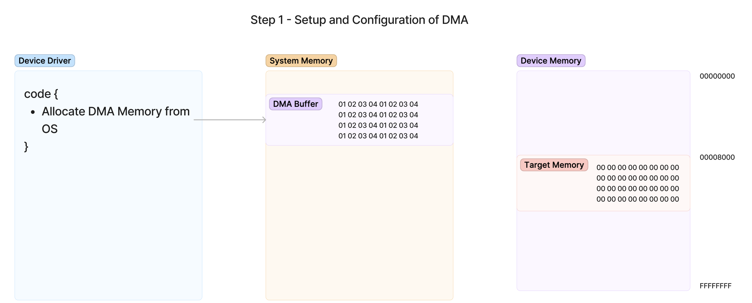
The first step of our DMA journey will be looking at the initial setup of the transfer. This involves a few steps that prepare the system memory, kernel, and device for the upcoming DMA transfer. In this case, we will be setting up DMA in order to read in the contents of memory in our DMA Buffer which is present in system RAM and place it into the device’s on-board RAM at Target Memory. We have already chosen at this point to read this memory from the DMA Buffer into address 0x8000 on the device. The goal is to transfer this memory as quickly as possible from system memory to the device so it can begin processing it. Assume in this case that the amount of memory is many megabytes and MMIO would be too slow, but we will only show 32 bytes of memory for simplicity. This transfer will be the simplest kind of DMA transfer: Copy a known size and address of a block of memory from system RAM into device RAM.
Step 1 - Allocating DMA Memory from the OS
The first step of this process is Allocate DMA Memory from OS. This means that the device driver must make an OS API call to ask the OS to allocate a region of memory for the device to write data to. This is important because the OS might need to perform special memory management operations to make the data available to the device, such as removing protections or reorganizing existing allocations to facilitate the request.
DMA memory classically must be contiguous physical memory, which means that the device starts at the beginning of some address and length and read/writes data linearly from the start to end of the buffer. Therefore, the OS must be responsible for organizing its physical memory to create contiguous ranges that are large enough for the DMA buffers being requested by the driver. Sometimes, this can be very difficult for the memory manager to do for a system that has been running for a very long time or has limited physical memory. Therefore, enhancements in this space have allowed more modern devices to transfer to non-contiguous regions of memory using features such as Scatter-Gather and IOMMU Remapping. Later on, we will look at some of those features. But for now, we will focus only on the simpler contiguous memory case.
Once the requested allocation succeeds, the memory address is returned by the API and points to the buffer in system RAM. This will be the address that the device will be able to access memory through DMA. The addresses returned by an API intended for DMA will be given a special name; device logical address or just logical address. For our example, a logical address is identical to a physical address. The device sees the exact same view of physical memory that our OS sees, and there are no additional translations done. However, this might not always be the case in more advanced forms of transfer. Therefore it’s best to be aware that a device address given to you might not always be the same as its actual physical address in RAM.
Once the buffer is allocated, since the intention is to move data from this buffer to the device, the device driver will populate the buffer in advance with the information it needs to write to the device. In this example, data made of a repeating 01 02 03 04 pattern is being transferred to the device’s RAM.
Step 2 - Programming DMA addresses to the device and beginning transfer
The next step of the transfer is to prepare the device with the information it needs to perform the transaction. This is usually where the knowledge of the device’s specific DMA interface is most important. Each device is programmed in its own way, and the only way to know how the driver should program the device is to either refer to its general standard such as the NVMe Specification or to simply work with the hardware designer.
In this example, I am going to make up a simplified DMA interface for a device with only the most barebones features necessary to perform a transfer. In the figures below, we can see that this device is programmed through values it writes into a BAR0 MMIO region. That means that to program DMA for this device, the driver must write memory into the MMIO region specified by BAR0. The locations of each register inside this BAR0 region are known in advance by the driver writer and is integrated into the device driver’s code.
I have created four device registers in BAR0 for this example:
- Destination Address - The address in the device’s internal RAM to write the data it reads from system RAM. This is where we will program our already-decided destination address of 0x8000.
- Source Address - The logical address of system RAM that the device will read data from. This will be programmed the logical address of our DMA Buffer which we want the device to read.
- Transfer Size - The size in bytes that we want to transfer.
- Initiate Transfer - As soon as a 1 is written to this register, the device will begin DMAing between the addresses given above. This is a way that the driver can tell that the device is done populating the buffer and is ready to start the transfer. This is commonly known as a doorbell register.
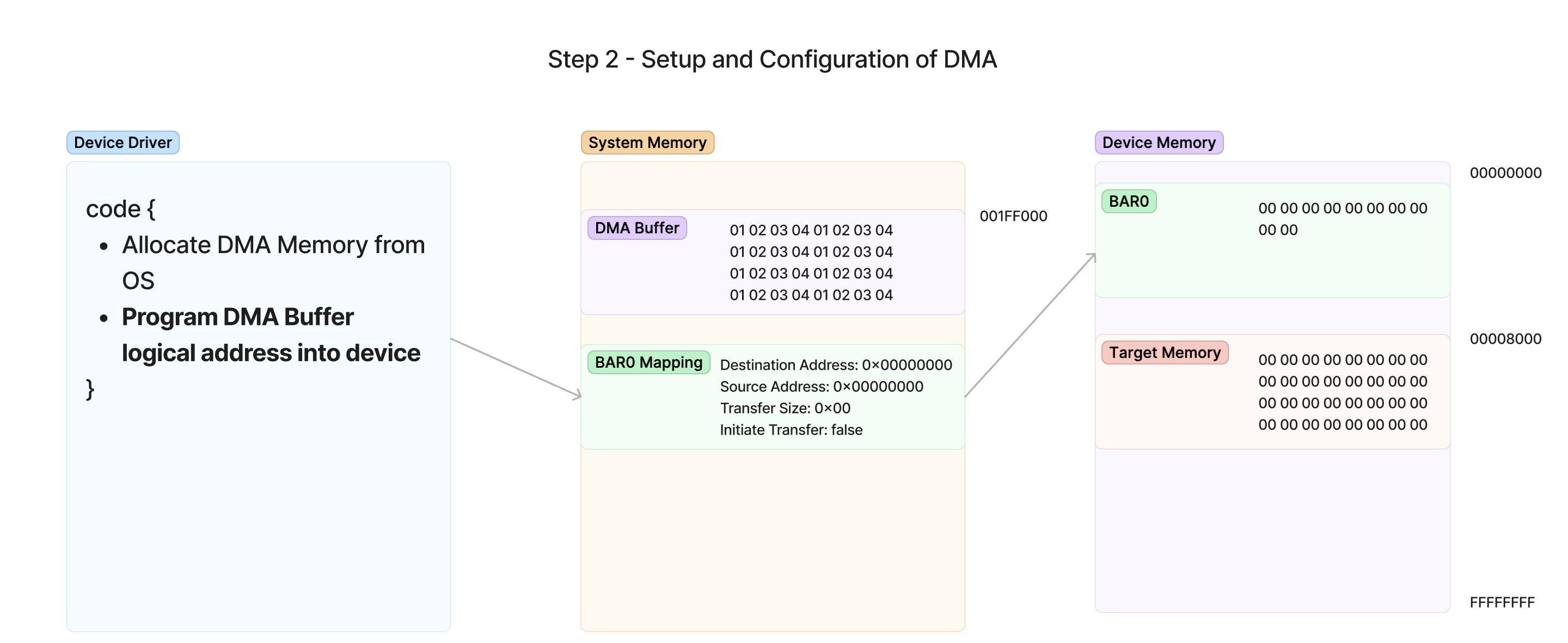
In the above diagram, the driver will need to write the necessary values into the registers using the mapped memory of BAR0 for the device (how it mapped this memory is dependent on the OS). The values in this diagram are as follows:
-
Target Memory - The memory we want to copy from the device will be at 0x00008000, which maps to a region of memory in the device’s on-board RAM. This will be our destination address.
-
DMA Buffer - The OS allocated the chunk of memory at 0x001FF000, so this will be our source address.
With this information, the driver can now program the values into the device as shown here:
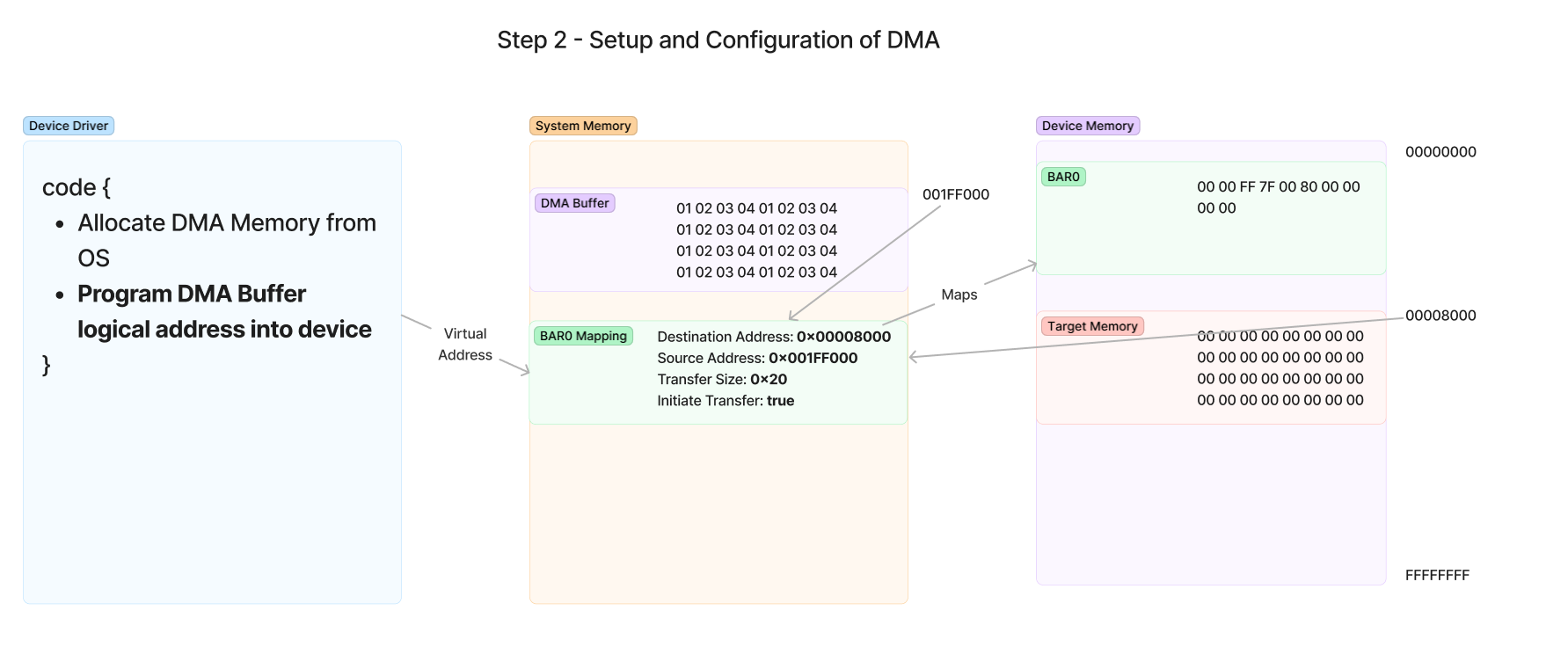
Now, at this point the driver has configured all the registers necessary to perform the transfer. The last step is to write a value to the Initiate Transfer register which acts as the doorbell register that begins the transfer. As soon as this value is written, the device will drive the DMA transfer and execute it independently of the driver or the CPU’s involvement. The driver has now completed its job of starting the transfer and now the CPU is free to do other work while it waits on the device to notify the system of the DMA completion.
Step 3 - Device performs DMA transaction
Now that the doorbell register has been written to by the driver, the device now takes over to handle the actual transfer. On the device itself, there exists a module called the DMA Engine responsible for handling and maintaining all aspects of the transaction. When the device was programmed, the register writes to BAR0 were programming the DMA engine with the information it needs to begin sending off the necessary TLPs on the PCIe link to perform memory transactions.
As discussed in a previous section, all memory operations on the PCIe link are done through Memory Write/Read TLPs. Here we will dive into what TLPs are sent and received by the DMA engine of the device while the transaction is taking place. Remember that it is easier to think of TLPs as network packets that are sending and receiving data on a single, reliable connection.
Interlude: Quick look into TLPs
Before we look at the TLPs on the link, let’s take a closer look at a high level overview of packet structure itself.
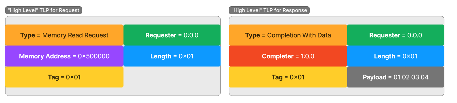
Here are two TLPs shown for a memory read request and response. As discussed, TLPs for memory operations utilize a request and response system. The device performing the read will generate a Read Request TLP for a specific address and length (in 4-byte DWORDs), then sit back and wait for the completion packets to arrive on the link containing the response data.
We can see there is metadata related to the device producing the request, the Requester, as well as a unique Tag value. This Tag value is used to match a request with its completion. When the device produces the request, it tags the TLP with a unique value to track a pending request. The value is chosen by the sender of the request, and it is up to the sender to keep track of the Tags it assigns.
As completions arrive on the link, the Tag value of the completion allows the device to properly move the incoming data to the desired location for that specific transfer. This system allows there to be multiple unique outstanding transfers from a single device that are receiving packets interleaved with each other but still remain organized as independent transfers.
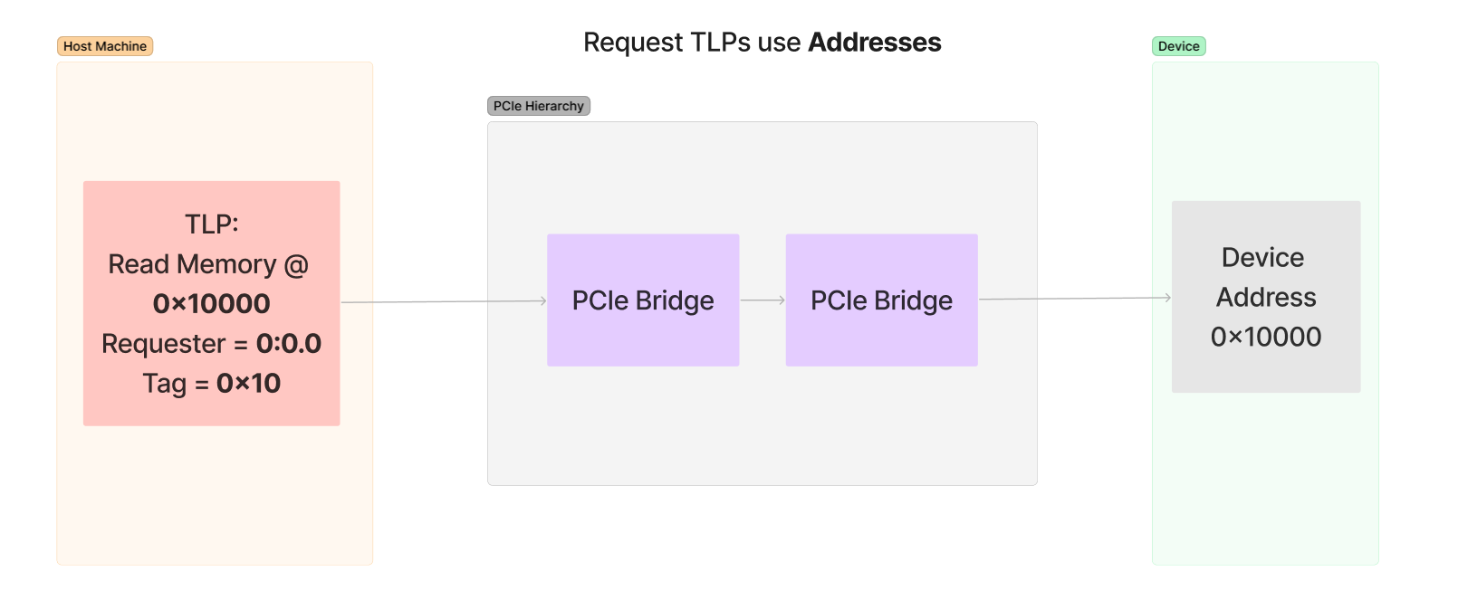
Also inside the packet is the information necessary to enable the PCIe switching hierarchy to determine where the request and completions need to go. For example, the Memory Address is used to determine which device is being requested for access. Each device in the hierarchy has been programmed during enumeration time to have unique ranges of addresses that each device owns. The switching hierarchy looks at the memory address in the packet to determine where that packet needs to go in order to access that address.
Once the device receives and processes the request, the response data is sent back in the form of a Completion TLP. The completion, or “response” packet, can and often will be fragmented into many smaller TLPs that send a part of the overall response. This is because there is a Maximum Payload Size (MPS) that was determined could be handled by the device and bus during enumeration time. The MPS is configurable based on platform and device capability and is a power of 2 size starting from 128 and going up to a potential 4096. Typically this value is around 256 bytes, meaning large read request will need to be split into many smaller TLPs. Each of these packets have a field that dictates what offset of the original request the completion is responding to and in the payload is the chunk of data being returned.
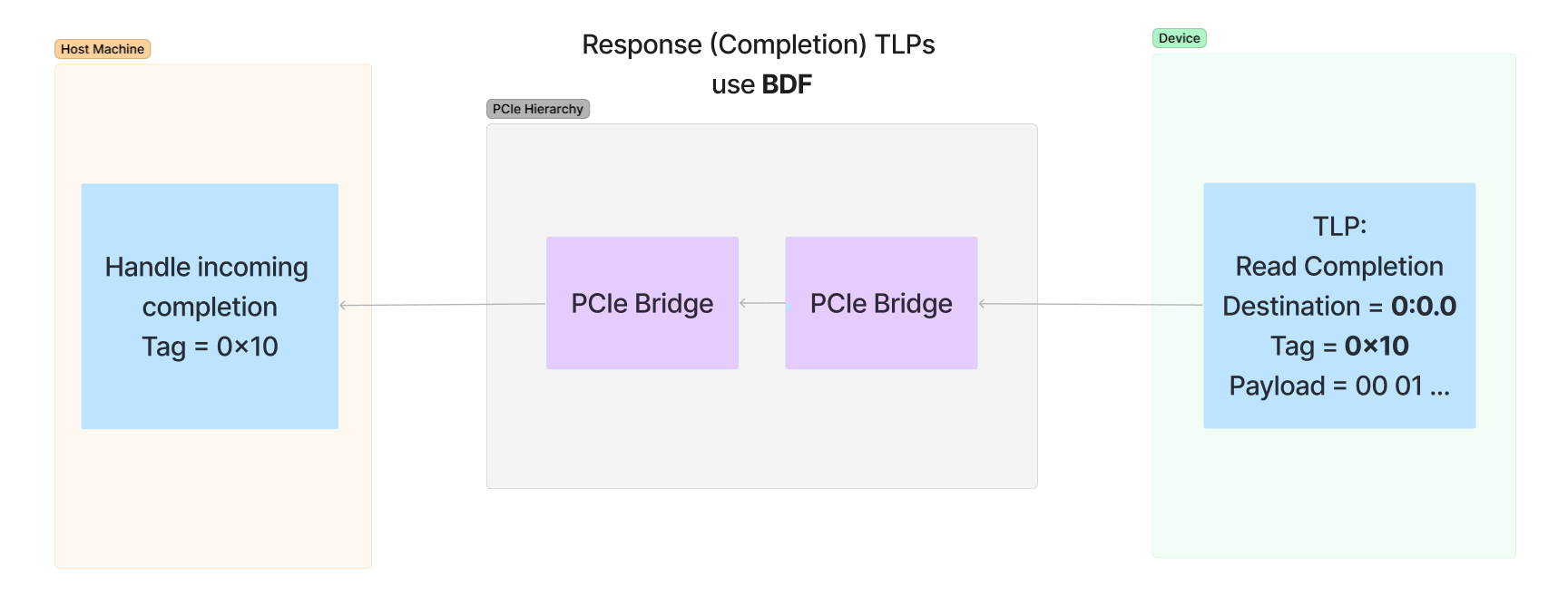
There is a common misconception that memory TLPs use BDF to address where packets need to go. The request uses only a memory address to direct a packet to its destination, and its the responsibility of the bridges in-between the device and destination to get that packet to its proper location. However, the completion packets do use the BDF of the Requester to return the data back to the device that requested it.
Below is a diagram of a memory read and response showcasing that requests use an address to make requests and completions use the BDF in the Requester field of the request to send a response:
Now back to the actual transaction…
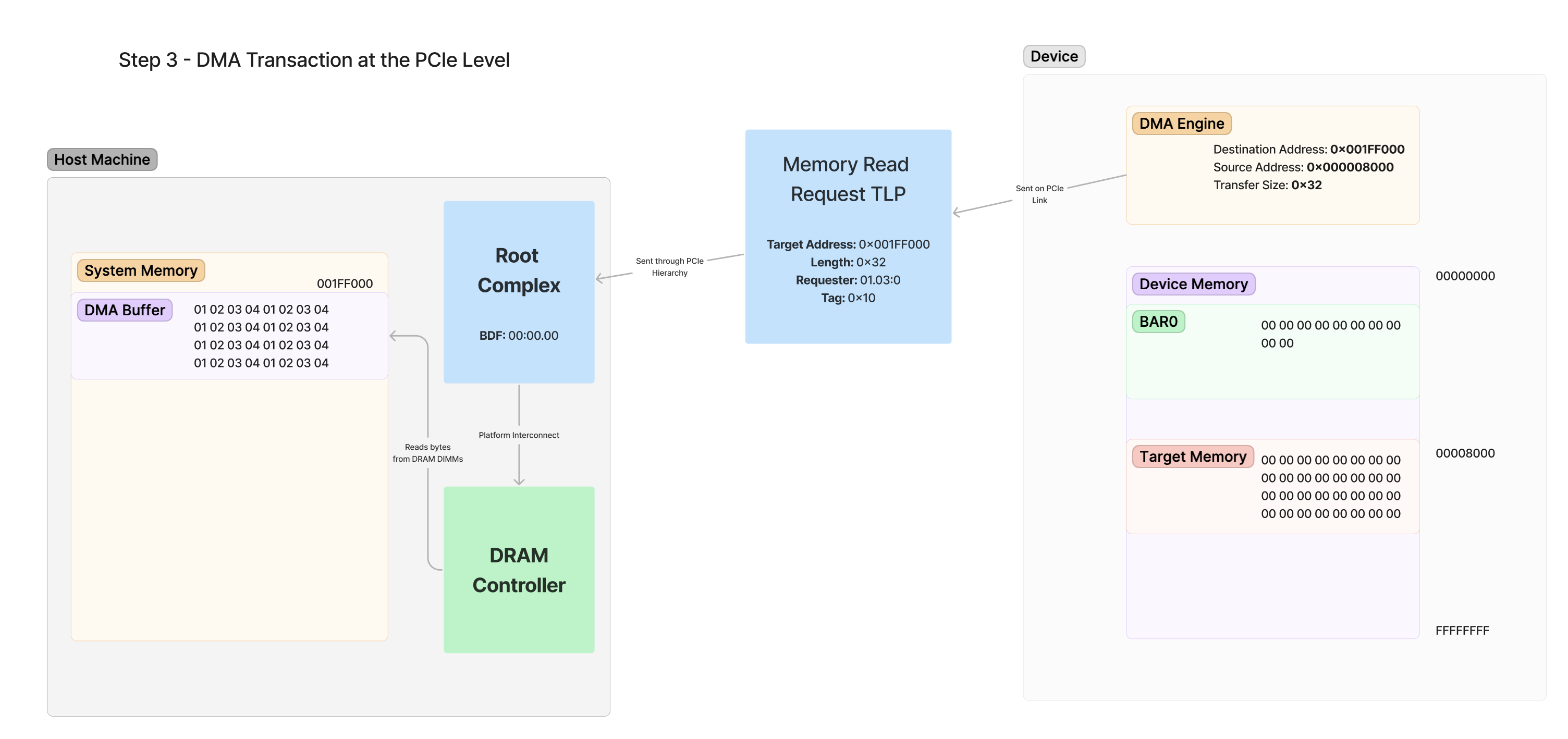
Let’s look at what all is sent and received by the DMA Engine in order to perform our request. Since we requested 32 bytes of data, there will only be one singular Memory Read Request and a singular Memory Read Completion packet with the response. For a small exercise for your understanding, stop reading forward and think for a moment which device is going to send and receive which TLP in this transaction. Scroll up above if you need to look at the diagrams of Step 2 again.
Now, let’s dig into the actual packets of the transfer. While I will continue to diagram this mock example out, I thought that for this exercise it might be fun and interesting to the reader to actually see what some of these TLPs look like when a real transaction is performed.
In the experiment, I set up the same general parameters as seen above with a real device and initiate DMA. The device will send real TLPs to read memory from system RAM and into the device. Therefore, you will be able to see a rare look into an example of the actual TLPs sent when performing this kind of DMA which are otherwise impossible to see in transit without one of these analyzers.
To view this experiment, follow this link to the companion post: Experiment - Packet Dumping PCIe DMA TLPs with a Protocol Analyzer and Pcileech
Here is a block diagram of the memory read request being generated by the device and how the request traverses through the hierarchy.
ERRATA: 0x32 should be 32
The steps outlined in this diagram are as follows:
- DMA Engine Creates TLP - The DMA engine recognizes that it must read 32 bytes from 0x001FF000. It generates a TLP that contains this request and sends it out via its local PCIe link.
- TLP Traverses Hierarchy - The switching hierarchy of PCIe moves this request through bridge devices until it arrives at its destination, which is the Root Complex. Recall that the RC is responsible for handling all incoming packets destined for accessing system RAM.
- DRAM Controller is Notified - The Root Complex internally communicates with the DRAM controller which is responsible for actually accessing the memory of the system DRAM.
- Memory is Read from DRAM - The given length of 32 bytes is requested from DRAM at address 0x001FF000 and returned to the Root Complex with the values 01 02 03 04…
Try your best not to be overwhelmed by this information, because I do understand there’s a lot going on just for the single memory request TLP. All of this at a high level is boiling down to just reading 32 bytes of memory from address 0x001FF000 in RAM. How the platform actually does that system DRAM read by communicating with the DRAM controller is shown just for your interest. The device itself is unaware of how the Root Complex is actually reading this memory, it just initiates the transfer with the TLP.
NOTE: Not shown here is the even more complicated process of RAM caching. On x86-64, all memory accesses from devices are cache coherent, which means that the platform automatically synchronizes the CPU caches with the values being accessed by the device. On other platforms, such as ARM platforms, this is an even more involved process due to its cache architecture. For now, we will just assume that the cache coherency is being handled automatically for us and we don’t have any special worries regarding it.
When the Root Complex received this TLP, it marked internally what the Requester and Tag were for the read. While it waits for DRAM to respond to the value, the knowledge of this request is pended in the Root Complex. To conceptualize this, think of this as an “open connection” in a network socket. The Root Complex knows what it needs to respond to, and therefore will wait until the response data is available before sending data back “over the socket”.
Finally, the Completion is sent back from the Root Complex to the device. Note the Destination is the same as the Requester:
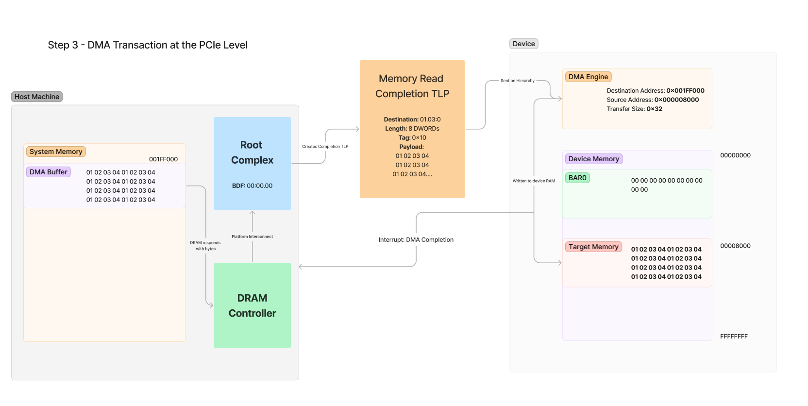
Here are the steps outlined with the response packet as seen above:
- Memory is read from DRAM - 32 bytes are read from the address of the DMA Buffer at 0x001FF000 in system DRAM by the DRAM controller.
- DRAM Controller Responds to Root Complex - The DRAM controller internally responds with the memory requested from DRAM to the Root Complex
- Root Complex Generates Completion - The Root Complex tracks the transfer and creates a Completion TLP for the values read from DRAM. In this TLP, the metadata values are set based on the knowledge that the RC has of the pending transfer, such as the number of bytes being sent, the Tag for the transfer, and the destination BDF that was copied from the Requester field in the original request.
- DMA Engine receives TLP - The DMA engine receives the TLP over the PCIe link and sees that the Tag matches the same tag of the original request. It also internally tracks this value and knows that the memory in the payload should be written to Target Memory, which is at 0x8000 in the device’s internal RAM.
- Target Memory is Written - The values in the device’s memory are updated with the values that were copied out of the Payload of the packet.
- System is Interrupted - While this is optional, most DMA engines will be configured to interrupt the host CPU whenever the DMA is complete. This gives the device driver a notification when the DMA has been successfully completed by the device.
Again, this is a lot of steps involved with handling just this single completion packet. However, again you can think of this whole thing as simply a “response of 32 bytes is received from the device’s request.” The rest of these steps are just to show you what a full end-to-end of this response processing would look like.
From here, the device driver is notified that the DMA is complete and the device driver’s code is responsible for cleaning up the DMA buffers or storing them away for use next time.
After all of this work, we have finally completed a single DMA transaction! And to think that this was the “simplest” form of a transfer I could provide. With the addition of IOMMU Remapping and Scatter-Gather Capability, these transactions can get even more complex. But for now, you should have a solid understanding of what DMA is all about and how it actually functions with a real device.
Outro - A Small Note on Complexity
If you finished reading this post and felt that you didn’t fully grasp all of the concepts thrown at you or feel overwhelmed by the complexity, you should not worry. The reason these posts are so complex is that it not only spans a wide range of topics, but it also spans a wide range of professions as well. Typically each part of this overall system has distinct teams in the industry who focus only on their “cog” in this complex machine. Often hardware developers focus on the device, driver developers focus on the driver code, and OS developers focus on the resource management. There’s rarely much overlap between these teams, except when handing off at their boundary so another team can link up to it.
These posts are a bit unique in that they try to document the system as a whole for conceptual understanding, not implementation. This means that where team boundaries are usually drawn, these posts simply do not care. I encourage readers who find this topic interesting to continue to dig into it on their own time. Maybe you can learn a thing about FPGAs and start making your own devices, or maybe you can acquire a device and start trying to reverse engineer how it works and communicate with it over your own custom software.
An insatiable appetite for opening black boxes is what the “hacker” mindset is all about!
Conclusion
I hope you enjoyed this deep dive into memory transfer on PCIe! While I have covered a ton of information in this post, the rabbit hole always goes deeper. Thankfully, by learning about config space access, MMIO (BARs), and DMA, you have now covered every form of data communication available in PCIe! For every device connected to the PCIe bus, the communication between the host system and device will take place with one of these three methods. All of the setup and configuration of a device’s link, resources, and driver software is to eventually facilitate these three forms of communication.
A huge reason this post took so long to get out there was due to just the sheer amount of information that I would have to present to a reader in order to make sense of all of this. It’s hard to decide what is worth writing about and what is so much depth that the understanding gets muddied. That decision paralysis has made the blog writing process take much longer than I intended. That, combined with a full time job, makes it difficult to find the time to get these posts written.
In the upcoming posts, I am looking forward to discussing some or all of the following topics:
- PCIe switching/bridging and enumeration of the hierarchy
- More advanced DMA topics, such as DMA Remapping
- Power management; how devices “sleep” and “wake”
- Interrupts and their allocation and handling by the platform/OS
- Simple driver development examples for a device
As always, if you have any questions or wish to comment or discuss an aspect of this series, you can best find me by “@gbps” in the #hardware channel on my discord, the Reverse Engineering discord: https://discord.com/invite/rtfm
Please look forward to future posts!
-Gbps