Introduction
In this post, I will be going over a small experiment where we hook up a PCIe device capable of performing arbitrary DMA to a Keysight PCIe 3.0 Protocol Analyzer to intercept and observe the Transaction Layer Packets (TLPs) that travel over the link. The purpose of this experiment is to develop a solid understanding of how memory transfer takes place under PCIe.
This is post is part of a series on PCIe for beginners. I encourage you to read the other posts before this one!
Background: On Why PCIe Hardware is so Unapproachable
There are a couple recurring themes of working with PCIe that make it exceptionally difficult for beginners: access to information and cost. Unlike tons of technologies we use today in computing, PCIe is mostly a “industry only” club. Generally, if you do not or have not worked directly in the industry with it, it is unlikely that you will have access to the information and tools necessary to work with it. This is not intentionally a gatekeeping effort as much as it is that the field serves a niche group of hardware designers and the tools needed to work with it are generally prohibitively expensive for a single individual.
The data transfer speeds that the links work near the fastest cutting-edge data transfer speeds available to the time period in which the standard is put into practice. The most recent standard of PCIe 6.2 has proof of concept hardware that operates at a whopping 64 GigaTransfers/s (GT/s) per lane. Each transfer will transfer one bit, so that means that a full 16 lane link is operating in total at a little over 1 Terabit of information transfer per second. Considering that most of our TCP/IP networks are still operating at 1 Gigabit max and the latest cutting-edge USB4 standards operates at 40 Gigabit max, that is still an order of magnitude faster than the transfer speeds we ever encounter in our day-to-day.
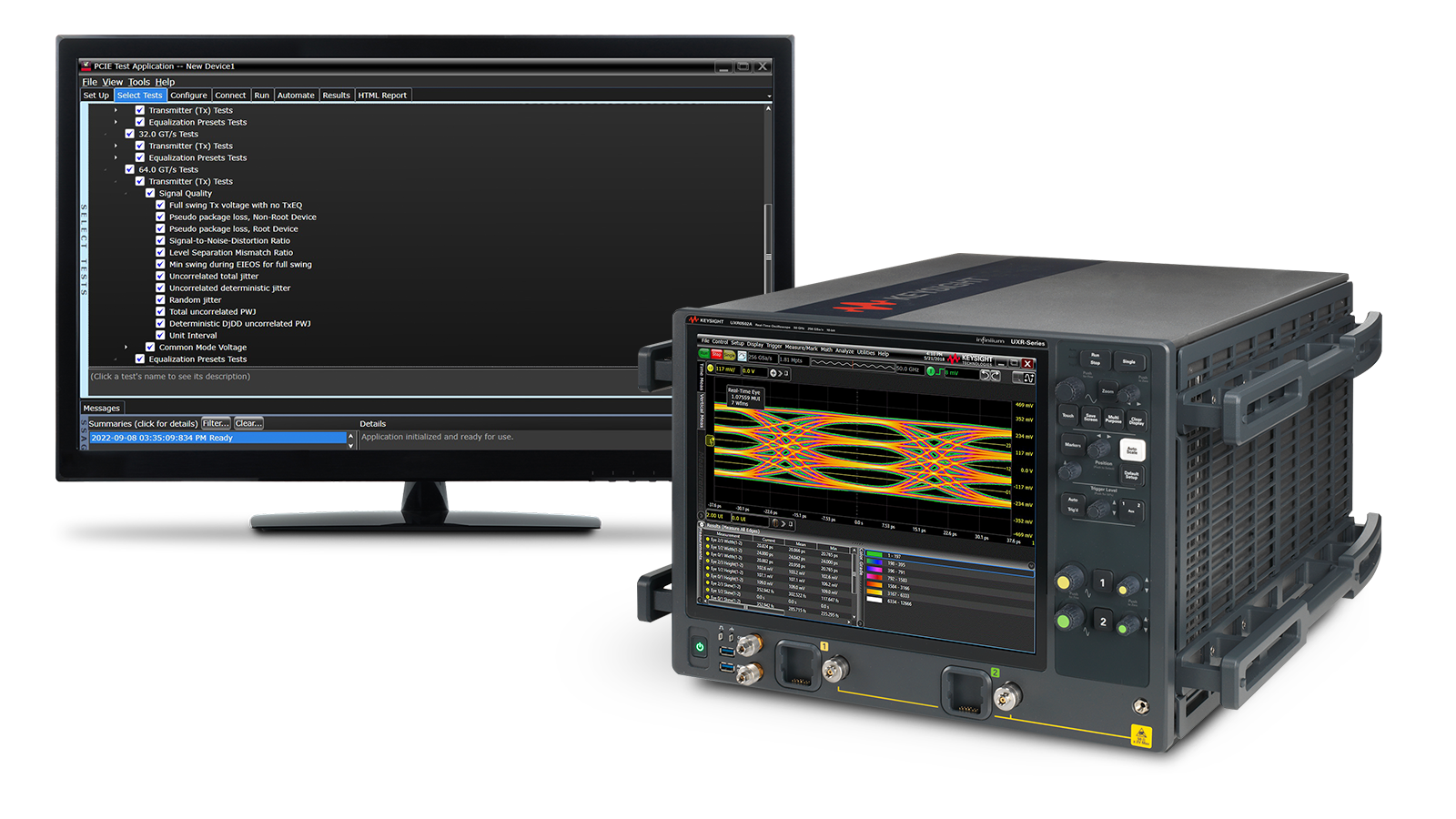
To build electronic test equipment, say an oscilloscope, that is capable of analyzing the electrical connection of a 64GT/s serial link is an exceptional feat in 2024. These devices need to contain the absolute most cutting edge components, DACs, and FPGAs/ASICs being produced on the market to even begin to be able to observe the speed by which the data travels over a copper trace without affecting the signal. Cutting edge dictates a price, and that price easily hits many hundreds of thousands of USD quickly. Unless you’re absolutely flushed with cash, you will only ever see one of these in a hardware test lab at a select few companies working with PCIe links.
But, all is not lost. Due to a fairly healthy secondhand market for electronics test equipment and recycling, it is still possible for an individual to acquire a PCIe protocol interceptor and analyzer for orders of magnitude less than what they were sold for new. The tricky part is finding all of the different parts of the collective set that are needed. An analyzer device is not useful without a probe to intercept traffic, nor is it useful without the interface used to hook it up to your PC or the license to the software that runs it. All of these pieces unfortunately have to align to recreate a functioning device.
It should be noted that these protocol analyzers are special in that they can see everything happening on the link. They have the capability to analyze each of the three layers of the PCIe link stack: the Physical, Data Link, and Transaction layer. If you’re not specifically designing something focused within the Physical or Data Link layer, these captures are not nearly as important as the Transaction layer. It is impossible for a PC platform to “dump” PCIe traffic like network or USB traffic. The cost of adding such a functionality would well outweigh the benefit.
My New PCIe 3.0 Protocol Analyzer Setup
After a year or so of looking, I was finally lucky enough to find all of the necessary pieces for a PCIe 3.0 Protocol Analyzer on Ebay at the same time, so I took the risk and purchased each of these components for myself (for what I believe was a fantastic deal compared to even the used market). I believe I was able to find these devices listed at all because they were approaching about a decade old and, at max, support PCIe 3.0. As newer consumer devices on the market are quickly moving to 4.0 and above, I can guess that this analyzer was probably from a lab that has recently upgraded to a newer spec. This however does not diminish the usefulness of a 3.0 analyzer, as all devices of a higher spec are backwards compatible with older speeds and still a huge swath of devices on the market in 2024 are still PCIe 3.0. NVMe SSDs and consumer GFX cards have been moving to 4.0 for the enhanced speed, but they still use the same feature set as 3.0. Most newer features are reserved for the server space.
Finding historical pricing information for these devices and cards is nearly impossible. You pretty much just pay whatever the company listing the device wants to get rid of it for. It’s rare to find any basis for what these are really “worth”.
Here is a listing of my setup, with the exact component identifiers and listings that were necessary to work together. If you were to purchase one of these, I do recommend this setup. Note that cables and cards similar but not exactly the same identifiers might not be compatible, so be exact!
- Agilent/Keysight U4301A PCI Express Protocol Analyzer Module - $1,800 USD (bundled with below)
- This is the actual analyzer module from Agilent that supports PCIe 3.0. This device is similar to a 1U server that must rack into a U4002A Digital Tester Chassis or a M9502A Chassis.
- The module comes installed with its software license on board. You do not need to purchase a separate license for its functionality.
- I used the latest edition of Windows 11 for the software.
- This single module can support up to 8 lanes of upstream and downstream at the same time. Two modules in a chassis would be required for 16 lanes of upstream and downstream.
- https://www.keysight.com/us/en/product/U4301A/pcie-analyzer.html
- Agilent/Keysight U4002A Digital Tester Chassis - $1,800 USD (bundled with above)
- This is the chassis that the analyzer module racks into. The chassis has an embedded controller module on it at the bottom which will be the component that hooks up to the PC. This is in charge of controlling the U4301A module and collects and manages its data for sending back to the PC.
- One Stop Systems OSS Host PCIe Card 7030-30048-01 A - $8 USD
- The host card that slots into a PCIe slot on the host PC’s motherboard. The cord and card should be plugged in and the module powered on for at least 4 minutes prior to booting the host PC.
- Molex 74546-0403 PCIe x4 iPass Cable - $15.88 USD
- The cord that connects the embedded controller module in the chassis to the PC through the OSS Host PCIe card.
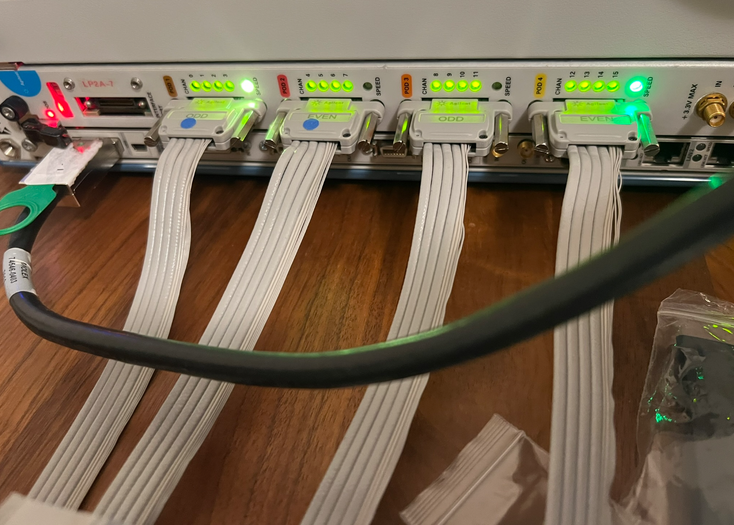
- Agilent/Keysight U4321 -66408 PCIe Interposer Probe Card With Cables And Adapter - $1,850 USD
- This is the interposer card that sits between the device under test and the slot on the target machine. This card is powered by a 12V DC power brick.
- This is an x8 card, so it can at the max support 8 lanes of PCIe. Devices under test will negotiate down to 8 lanes if needed, so this is not an isssue.
- https://www.keysight.com/us/en/product/U4321A/pcie-interposer-probe.html
-
At least 2x U4321-61601 Solid Slot Interposer Cables are needed to attach to the U4321. 4x are needed for bidirectional x8 connection. These were bundled along with the above.
- Total Damage: Roughly ~$4000 USD.
FPGA Setup for DMA with Pcileech
It’s totally possible to connect an arbitrary PCIe device, such as a graphics card, and capture its DMA for this experiment. However, I think it’s much nicer to create the experiment by being able to issue arbitrary DMA from a device and observing its communication under the analyzer. That way there’s not a lot of chatter from the regular device’s operation happening on the link that affects the results.
For this experiment, I’m using the fantastic Pcileech project. This project uses a range of possible Xilinx FPGA boards to perform arbitrary DMA operations with a target machine through the card. The card hooks up to a sideband host machine awaiting commands and sends and receives TLPs over a connection (typically USB, sometimes UDP) to the FPGA board that eventually gets sent/received on the actual PCIe link. Basically, this project creates a “tunnel” from PCIe TLP link to the host machine to perform DMA with a target machine.
If you are not aware, FPGA stands for Field-Programmable Gate Array. It is essentially a chip that can have all of its digital logic elements reprogrammed at runtime. This allows a hardware designer to create and change high speed hardware designs on the fly without having to actually create a custom silicon chip, which can easily run in the millions of USD. The development boards for these FPGAs start at about $200 for entry level boards and typically have lots of high and low speed I/O interfaces that the chip could be programmed to communicate to. Many of these FPGA boards support PCIe, so this is a great way to work with high speed protocols that cannot be handled by your standard microcontroller.
FPGAs are a very difficult space to break into. For a beginner book on FPGAs, I highly recommend this new book from No Starch (Russell Merrick): Getting Started with FPGAs. However, to use the Pcileech project, you can purchase one of the boards listed under the project compatibility page on GitHub and use it without any FPGA knowledge.
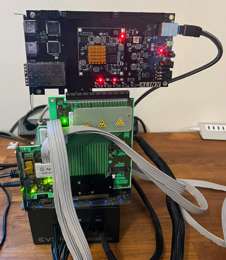
For my project, I am using my Alinx AX7A035 PCIe 2.0 Development Board. This is a surprisingly cheap PCIe-capable FPGA board, and Alinx has proven to me to be a fantastic company to work with as an individual. Their prices are super reasonable for their power, the company provides vast documentation of their boards and schematics, and they also provide example projects for all of the major features of the board. I highly recommend their boards to anyone interested in FPGAs.
While the pcileech project does not have any support the AX7A035 board, it does have support for the same FPGA as the one used on the AX7A035. I had to manually port the project to this Alinx board myself by porting the HDL. Hopefully this port will provide interested parties with a cheap alternative board to the ones supported by the pcileech project as is.
In the project port, the device is ported to use Gigabit Ethernet to send and receive the TLPs instead of USB3. Gigabit Ethernet operates at about 32MB/s of memory for pcileech memory dumping, which is fairly slow compared to the speeds of USB 3.0 achieved by other pcileech devices (130MB/s). However, the board does not have a FT601 USB 3.0 chip to interface with, so the next fastest thing I can easily use on this board is Ethernet.
In this DMA setup, I have the Ethernet cord attached to the system the device is attacking. This means the system can send UDP packets to perform DMA with itself.
Link will be available soon to the ported design on my GitHub.
Experiment - Viewing Configuration Space Packets
For more information about TLPs, please see Part 1 and Part 2 of my PCIe blog post series.
The first part of this experiment will be viewing what a Configuration Read Request (CfgRd) packet looks like under the analyzer. The target machine is a basic Ubuntu 22.04 Server running on a Zen 3 Ryzen 5 platform. This version of the OS does not have IOMMU support for AMD and therefore does not attempt to protect any of its memory. There is nothing special about the target machine other than the FPGA device plugged into it.
The first command we’re going to execute is the lspci command, which is a built-in Linux command used to list PCI devices connected to the system. This command provides a similar functionality to what Device Manager on Windows provides.
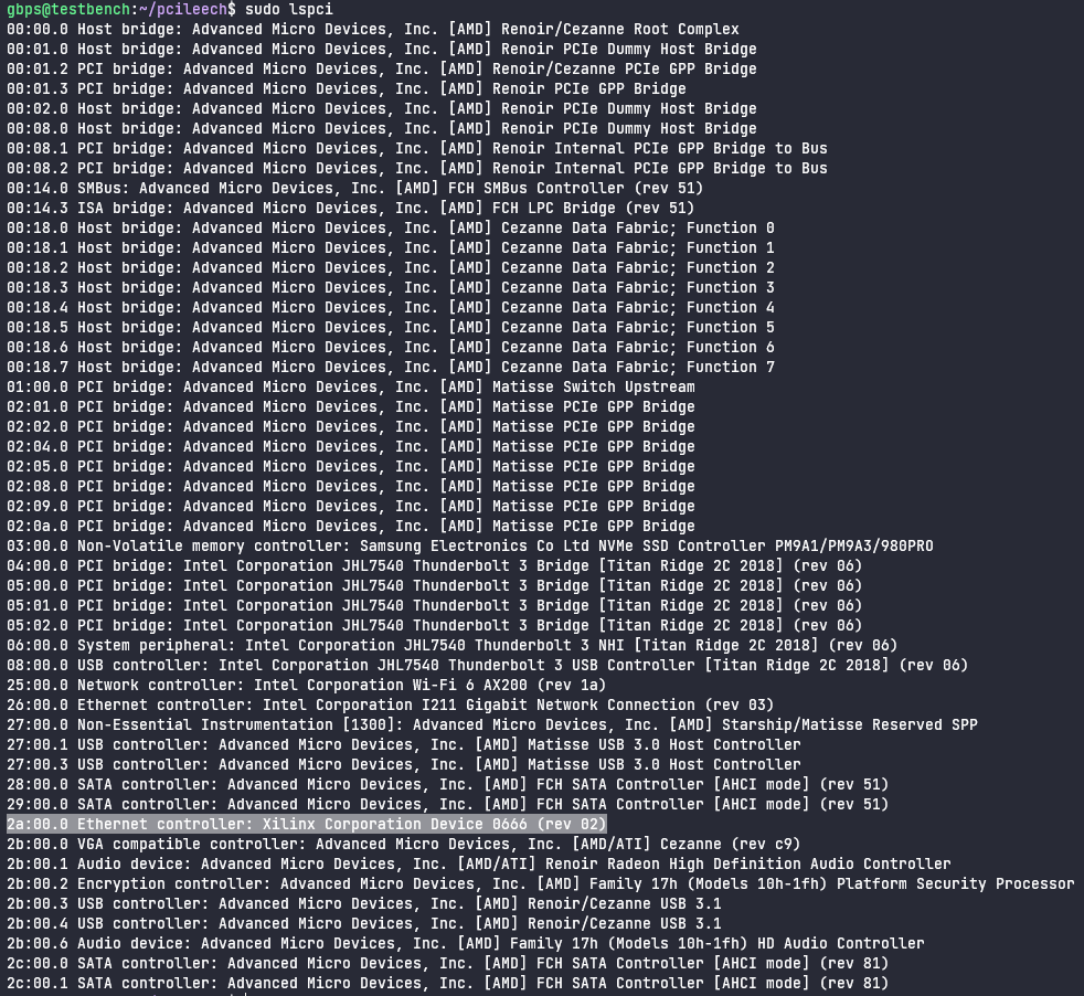
Using this command, we can find that the pcileech device is located at BDF 2a:00.0. This is bus 2a, device 00, and function 0.
The next command to execute is sudo lspci -vvv -s 2a:00.0 which will dump all configuration space for the given device.
-vvvmeans maximum verbosity. We want it to dump all information it can about configuration space.-s 2a:00.0means only dump the configuration space of the device with BDF2a:00.0, which we found above.
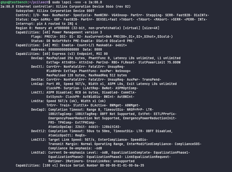
Here we see a full printout of all of the details of the individual bits of each of the Capabilities in configuration space. We can also see that this pcileech device is masquerading as a Ethernet device, despite not providing any Ethernet functionality.
Now, let’s prepare the protocol analyzer to capture the CfgRd packets from the wire. This is done by triggering on TLPs sent over the link and filtering out all Data Link and Physical Layer packets that we do not care to view.
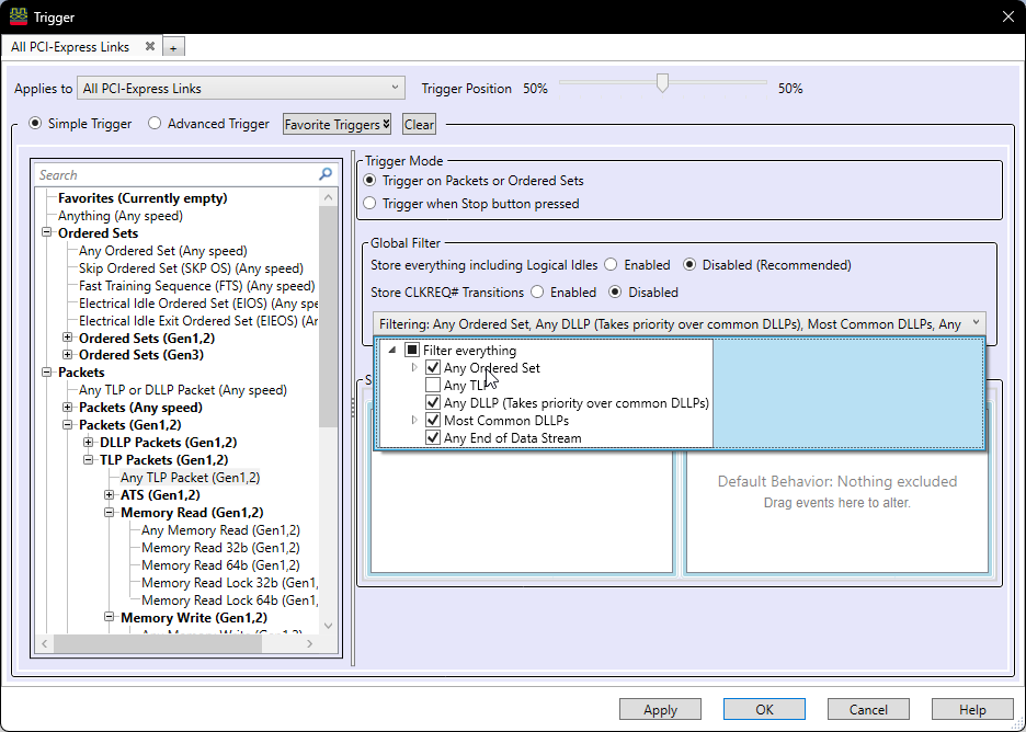
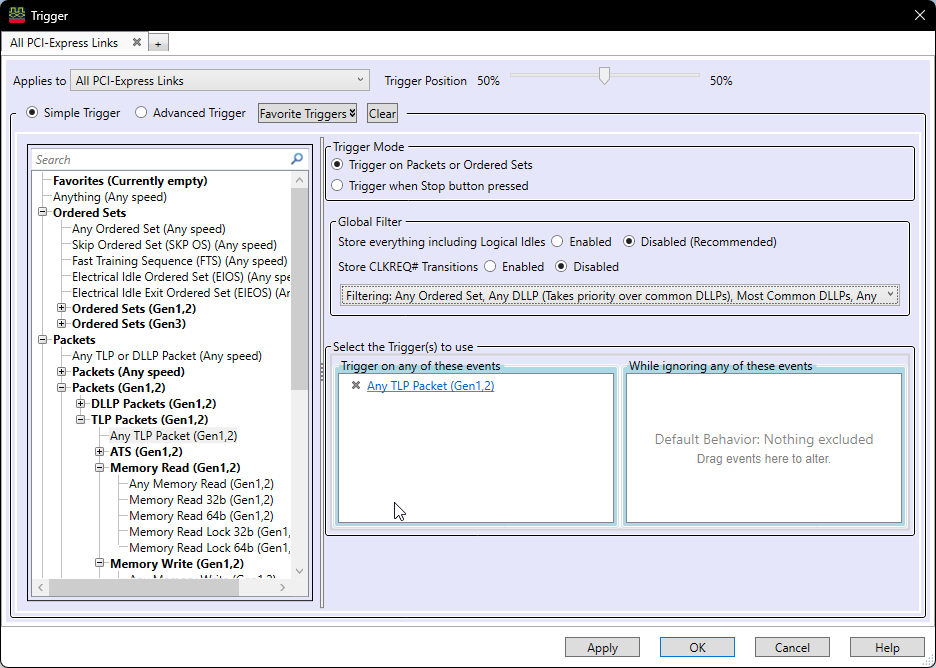
With this set up, we can run the analyzer and wait for it to trigger on a TLP being sent or received. In this case, we are expecting the target machine to send CfgRd TLPs to the device to read its configuration space. The device is expected to respond with Completions with Data TLPs (CplD TLPs) containing the payload of the response to the configuration space read.
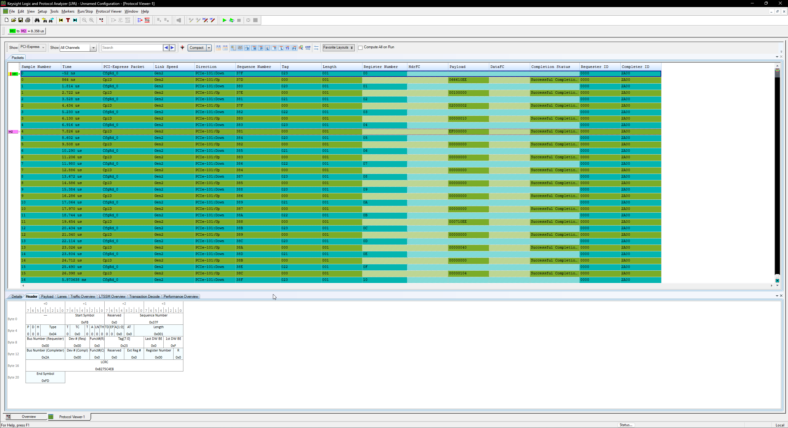

In the above packet overview, we can see a few interesting properties of the packets listed by the analyzer.
- We can see the CfgRd_0 packet is going Downstream (host -> device)
- We can see the CplD for the packet is going Upstream (device -> host)
- Under Register Number we see the offset of the 4-byte DWORD being read
- Under Payload we can see the response data. For offset 0, this is the Vendor ID (2bytes) and Device ID (2bytes). 10EE is the vendor ID for Xilinx and 0666 is a the device id of the Ethernet device, as seen above in the lspci output.
- We can see it was a Successful Completion.
- We can see the Requester ID was 00:00.0 which is the Root Complex.
- We can see the Completer ID was 1A:00.0 which is the Device.
Cool! Now let’s look at the individual packet structures of the TLPs themselves:
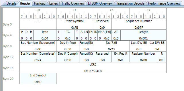
Here we can see the structure of a real TLP generated from the AMD Root Complex and going over the wire to the FPGA DMA device. There are a few more interesting fields now to point out:
-
Type: 0x4 is the type ID for CfgRd_0.
- Sequence Number: The TLP sent over the link has a sequence number associated that starts at 0x00 and increments by 1. The TLP is acknowledged by the receiver after successfully being sent using an Ack Data-Link Layer packet (not shown). This ensures every packet is acknowledge as being received.
- Length: The Length field of this packet is set to 0x01, which means it wants to read 1 DWORD of configuration space.
- Tag: The Tag is set to 0x23. This means that the Completion containing the data being read from config space must respond with the Tag of 0x23 to match up the request and response.
- Register Number: We are reading from offset 0x00 of config space.
- **Requester and Completer: **Here we can see that the packet is marked with the sender and receiver BDFs. Remember that config space packets are sent to BDFs directly!
Finally, let’s look at the structure of the Completion with Data (CplD) for the CfgRd request.
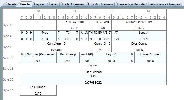
This is the response packet immediately sent back by the device responding to the request to read 4 bytes at offset 0.
Here are the interesting fields to point out again:
-
Type: 0x0A is the type for Completion
- The TLP contains Payload Data, so the Data Attr Bit (D) is set to 1.
- The Completer and Requester IDs remain the same. The switching hierarchy knows to return Completions back to their requester ID.
- The Tag is 0x23, which means this is the completion responding to the above packet.
- This packet has a Payload of 1 DWORD, which is 0xEE106606. When read as two little endian 2-byte values, this is 0x10EE and 0x0666.
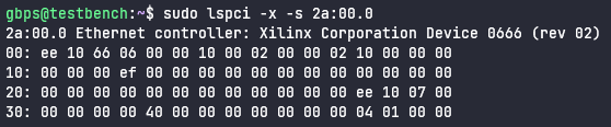
We can also verify the same bytes of data were returned through a raw hex dump of config space:
Experiment - Performing and Viewing DMA to System RAM
Setup
For the final experiment, let’s do some DMA from our FPGA device to the target system! We will do this by using pcileech to send a request to read an address and length and observing the resulting data from RAM sent from the AMD Zen 3 system back to the device.
The first step is to figure out where the device is going to DMA to. Recall in the Part 2 post that the device is informed by the device driver software where to DMA to and from. In this case, our device does not have a driver installed at all for it. In fact, it is just sitting on the PCI bus after enumeration and doing absolutely nothing until commanded by the pcileech software over the UDP connection.
To figure out where to DMA to, we can dump the full physical memory layout of the system using the following:
gbps@testbench:~/pcileech$ sudo cat /proc/iomem
00001000-0009ffff : System RAM
  00000000-00000000 : PCI Bus 0000:00
  000a0000-000dffff : PCI Bus 0000:00
    000c0000-000cd7ff : Video ROM
  000f0000-000fffff : System ROM
00100000-09afefff : System RAM
0a000000-0a1fffff : System RAM
0a200000-0a20cfff : ACPI Non-volatile Storage
0a20d000-69384fff : System RAM
  49400000-4a402581 : Kernel code
  4a600000-4b09ffff : Kernel rodata
  4b200000-4b64ac3f : Kernel data
  4b9b9000-4cbfffff : Kernel bss
69386000-6a3edfff : System RAM
6a3ef000-84ab5017 : System RAM
84ab5018-84ac2857 : System RAM
84ac2858-85081fff : System RAM
850c3000-85148fff : System RAM
8514a000-88caefff : System RAM
  8a3cf000-8a3d2fff : MSFT0101:00
    8a3cf000-8a3d2fff : MSFT0101:00
  8a3d3000-8a3d6fff : MSFT0101:00
    8a3d3000-8a3d6fff : MSFT0101:00
8a3f0000-8a426fff : ACPI Tables
8a427000-8bedbfff : ACPI Non-volatile Storage
8bedc000-8cffefff : Reserved
8cfff000-8dffffff : System RAM
8e000000-8fffffff : Reserved
90000000-efffffff : PCI Bus 0000:00
  90000000-b3ffffff : PCI Bus 0000:01
    90000000-b3ffffff : PCI Bus 0000:02
      90000000-b3ffffff : PCI Bus 0000:04
        90000000-b3ffffff : PCI Bus 0000:05
          90000000-901fffff : PCI Bus 0000:07
  c0000000-d01fffff : PCI Bus 0000:2b
    c0000000-cfffffff : 0000:2b:00.0
    d0000000-d01fffff : 0000:2b:00.0
  d8000000-ee9fffff : PCI Bus 0000:01
    d8000000-ee9fffff : PCI Bus 0000:02
      d8000000-ee1fffff : PCI Bus 0000:04
        d8000000-ee1fffff : PCI Bus 0000:05
          d8000000-d80fffff : PCI Bus 0000:08
          d8000000-d800ffff : 0000:08:00.0
          d8000000-d800ffff : xhci-hcd
          d8100000-d82fffff : PCI Bus 0000:07
          ee100000-ee1fffff : PCI Bus 0000:06
          ee100000-ee13ffff : 0000:06:00.0
          ee100000-ee13ffff : thunderbolt
          ee140000-ee140fff : 0000:06:00.0
      ee300000-ee4fffff : PCI Bus 0000:27
        ee300000-ee3fffff : 0000:27:00.3
          ee300000-ee3fffff : xhci-hcd
        ee400000-ee4fffff : 0000:27:00.1
          ee400000-ee4fffff : xhci-hcd
      ee500000-ee5fffff : PCI Bus 0000:29
        ee500000-ee5007ff : 0000:29:00.0
          ee500000-ee5007ff : ahci
      ee600000-ee6fffff : PCI Bus 0000:28
        ee600000-ee6007ff : 0000:28:00.0
          ee600000-ee6007ff : ahci
      ee700000-ee7fffff : PCI Bus 0000:26
        ee700000-ee71ffff : 0000:26:00.0
          ee700000-ee71ffff : igb
        ee720000-ee723fff : 0000:26:00.0
          ee720000-ee723fff : igb
      ee800000-ee8fffff : PCI Bus 0000:25
        ee800000-ee803fff : 0000:25:00.0
          ee800000-ee803fff : iwlwifi
      ee900000-ee9fffff : PCI Bus 0000:03
        ee900000-ee903fff : 0000:03:00.0
          ee900000-ee903fff : nvme
  eeb00000-eeefffff : PCI Bus 0000:2b
    eeb00000-eebfffff : 0000:2b:00.4
      eeb00000-eebfffff : xhci-hcd
    eec00000-eecfffff : 0000:2b:00.3
      eec00000-eecfffff : xhci-hcd
    eed00000-eedfffff : 0000:2b:00.2
      eed00000-eedfffff : ccp
    eee00000-eee7ffff : 0000:2b:00.0
    eee80000-eee87fff : 0000:2b:00.6
      eee80000-eee87fff : ICH HD audio
    eee88000-eee8bfff : 0000:2b:00.1
      eee88000-eee8bfff : ICH HD audio
    eee8c000-eee8dfff : 0000:2b:00.2
      eee8c000-eee8dfff : ccp
  eef00000-eeffffff : PCI Bus 0000:2c
    eef00000-eef007ff : 0000:2c:00.1
      eef00000-eef007ff : ahci
    eef01000-eef017ff : 0000:2c:00.0
      eef01000-eef017ff : ahci
  ef000000-ef0fffff : PCI Bus 0000:2a
    ef000000-ef000fff : 0000:2a:00.0
f0000000-f7ffffff : PCI MMCONFIG 0000 [bus 00-7f]
    f0000000-f7ffffff : pnp 00:00
  fd210510-fd21053f : MSFT0101:00
  feb80000-febfffff : pnp 00:01
  fec00000-fec003ff : IOAPIC 0
  fec01000-fec013ff : IOAPIC 1
  fec10000-fec10fff : pnp 00:05
  fed00000-fed003ff : HPET 0
    fed00000-fed003ff : PNP0103:00
  fed81200-fed812ff : AMDI0030:00
  fed81500-fed818ff : AMDI0030:00
fedc0000-fedc0fff : pnp 00:05
fee00000-fee00fff : Local APIC
  fee00000-fee00fff : pnp 00:05
  ff000000-ffffffff : pnp 00:05
100000000-24e2fffff : System RAM
  250000000-26fffffff : pnp 00:02
3fffe0000000-3fffffffffff : 0000:2b:00.0
Reserved regions removed for brevity.
In this case, for this experiment, I am going to read 0x1000 bytes (one 4096 byte page) of memory from the 32-bit address 0x10000 which begins the first range of System RAM assigned to the physical address layout:
00001000-0009ffff : System RAM
Since this is actual RAM, our DMA will be successful. If this was not memory, our request would likely receive a Completion Error with Unsupported Request.
The pcileech command to execute will be:
sudo pcileech -device rawudp://ip=10.0.0.64 dump -min 0x1000 -max 0x2000
Where:
- The FPGA device is assigned the IP address
10.0.0.64by my LAN dumpis the command to execute-min 0x1000specifies to start dumping memory from this address-max 0x2000specifies to stop dumping memory at this address. This results in 0x1000 bytes being read from the device.
Analyzer Output
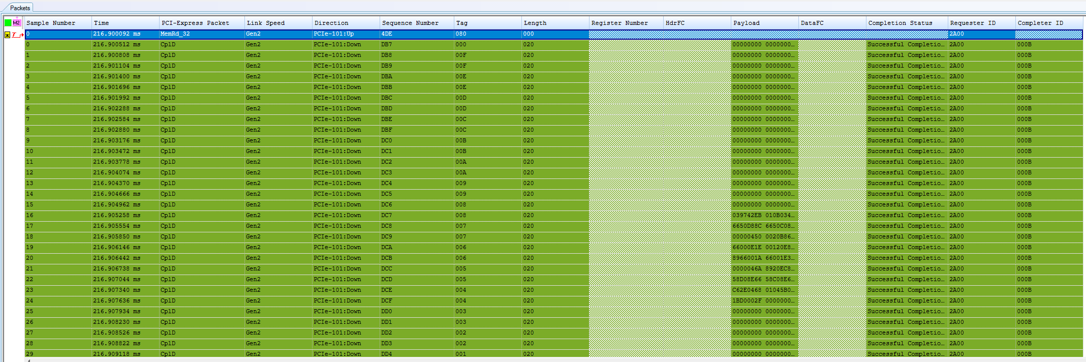
From this output, you can see an interesting property of DMA: the sheer number of packets involved. The first packet here is a MemRd_32 packet headed upstream. If the address being targeted was a 64-bit address, it would use the MemRd_64 TLP. Let’s take a look at that first:
Here we can see a few interesting things:
- The Requester field contains the device’s BDF. This is because the device initiated the request, not the Root Complex.
- The Address is 0x1000. This means we are requesting to read from address 0x1000 as expected.
- The Length is 0x000, which is the number of 4-byte DWORDs to transfer. This seems a bit weird, because we are reading 4096 bytes of data. This is actually because 0x000 is a special number that means Maximum Length. In the above bit layout, we see the Length field in the packet is 9 bits. The maximum 9 bit value that can be expressed in binary is
0x3FF.0x3FF * 4 = 0xFFCwhich is 4 bytes too small to express the number 4096. Since transferring 0 bytes of data doesn’t make sense, the number is used to indicate the maximum value, or 4096 in this case! - The Tag is 0x80. We will expect all Completions to also have the same Tag to match the response to the request.
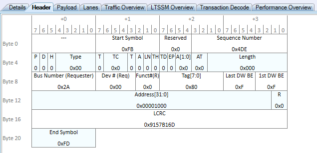
And finally, let’s look at the first Completion with Data (CplD) returned by the host:
We can see right off the bat that this looks a whole lot like a Completion with Data for the config space read in the previous section. But in this case, it’s much larger in size, containing a total of 128 bytes of payload returned from System RAM to our device.
Some more interesting things to point out here:
- Length: Length is 0x20 DWORDs, or 0x20*4=128 bytes of payload. This means that the resulting 4096 byte transfer has been split up into many CplD TLPs each containing 128 bytes of the total payload.
- Byte Count: This value shows the remaining number of DWORDs left to be sent back for the request. In this case, it is 0x000 again, which means that this is the first of 4096 bytes pending.
- Tag: The Tag of 0x80 matches the value of our request.
- Requester ID: This Completion found its way back to our device due to the 2A:00.0 address being marked in the requester.
- Completer ID: An interesting change here compared to config space, but the Completer here is not the 00:00.0 Root Complex device. Instead, it is a device 00:01.3. What device is that? If we look back up at the lspci output, this is a Root Port bridge device. It appears that this platform marks the Completer of the request as the Root Port the device is connected to, not the Root Complex itself.
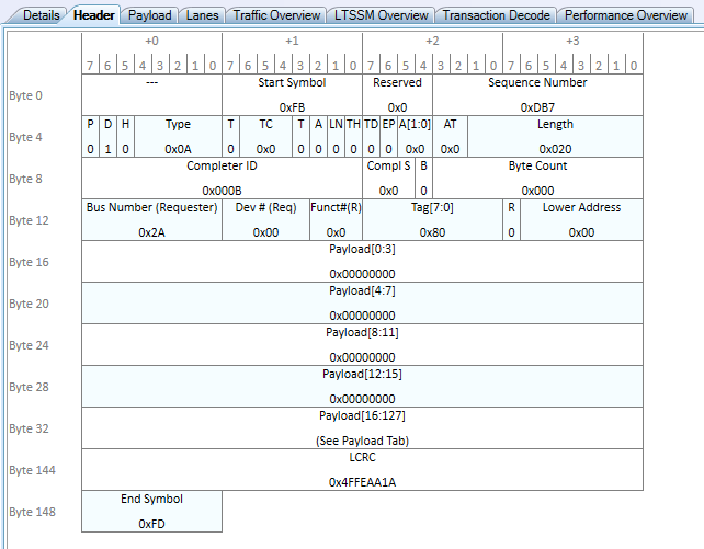
And just for consistency, here is the second Completion with Data (CplD) returned by the host:
The major change here for the second chunk of 128 bytes of payload is that the Byte Count field has decremented by 0x20, which was the size of the previous completion. This means that this chunk of data will be read into the device at offset 0x20*4 = 0x80. This shouldn’t be too surprising, we will continue to decrement this Byte Count field until it eventually reaches 0x020, which will mark the final completion of the transfer. The DMA Engine on the device will recognize that the transfer is complete and mark the original 4096 byte request as complete internally.
gbps@testbench:~/pcileech$ sudo pcileech -device rawudp://ip=10.0.0.64 dump -min 0x1000 -max 0x2000

 Current Action: Dumping Memory
 Access Mode:    Normal
 Progress:       0 / 0 (100%)
 Speed:          4 kB/s
 Address:        0x0000000000001000
 Pages read:     1 / 1 (100%)
 Pages failed:   0 (0%)
Memory Dump: Successful.
Maximum Payload Size Configuration
Now only one question remains, why are there so many Completion TLPs for a single page read?
The answer lies in a specific configuration property of the device and the platform: the Maximum Payload Size.
If we look back at the configuration space of the device:
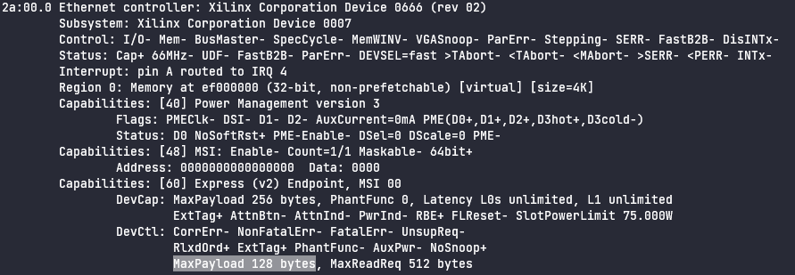
The Device Control register has been programmed with a MaxPayload of 128 bytes. This means that the device is not allowed to send or receive any TLP with a payload larger than 128 bytes. This means that our 4096 byte request will always be fragmented into 4096/128 = 32 completions per page.
If you notice above, there is a field DevCap: MaxPayload 256 bytes that dictates that the Device Capabilities register is advertising this device’s hardware is able to handle up to 256 bytes. So if this device supports up to 256 byte payloads, that means the device could potentially cut the TLP header overhead in half to only 16 completions per page.
It is not clear what from the platform or OS level at this exact moment has reduced the MaxPayload to 128 bytes. Typically it is the bridge device above the device in question that limits the MaxPayload size, however in this case the max size supported by the Root Port this device is connected to is 512 bytes. With some further investigation, maybe I’ll be able to discover that answer.
And there you have it, a more in-depth look into how a device performs DMA!
Conclusion
This simple experiment hopefully gives you a nicer look into the “black box” of the PCIe link. While it’s nice to see diagrams, I think it’s much sweeter to look into actual packets on the wire to confirm that your understanding is what actually happens in practice.
We saw that config space requests are simple 4-byte data accesses that utilize the CfgRd and CfgWr TLP types. This is separate from DMA or MMIO, which uses the MemRd/MemWr that are used in DMA and MMIO. We also saw how the Completions can be fragmented in order to return parts of the overall transfer for larger DMA transfers such as the 4096 page size.
I hope to provide more complex or potentially more “interactive” experiments later. For now, I leave you with this as a more simplistic companion to the Part 2 of my series.
Hope you enjoyed!
- Gbps