Foreword about the series
Hello! I have been speaking to some friends and coworkers lately interested in learning more about PCIe but feeling intimidated by the complexity or the lack of simple resources for beginners. I have been working with PCIe a lot lately and felt like it might be worth sharing some of my experience in the form of a blog post.
This post is intended to be utilized by those with a background with computer systems who like to get their hands dirty. It is also intended for total beginners to PCIe or someone who is aware of the general concepts but is having trouble linking the concepts together.
First thing’s first: Do not be intimidated. There are a lot of acronyms and confusing concepts that will be made simple as you “get it”. Take things a step at the time and don’t be afraid to ask questions! (If you want to ask me questions, consider pinging me @Gbps in the #hardware channel in the Reverse Engineering Discord)
I intend to do a couple of things with this series:
- Break PCIe down into what I feel is most important from the software side to learn and build a good baseline mental model for modern PC/server systems.
- Show practical examples of investigating PCIe hierarchies and devices on Windows using various tools (usually WinDbg).
- I will hand wave or omit some specific details intentionally to avoid confusion. Terminology here may be incorrect, even the information itself might be technically incorrect. But the purpose of this is to learn the system as a whole, not the specific details of the specification. PCIe is complex, and it is not worth getting caught up in too many details and corner-cases when building a beginner’s understanding.
- Hopefully demystify this technology by relating it back to concepts you are already familiar with. PCIe did not re-invent the wheel, and you probably understand a lot more about it already than you realize by understanding technologies similar to it.
I do not intended to do the following things with this series:
- Go into detail about legacy PCI or PCI-X. This technology is, in general, not important other than for historical interest.
- Show you how to write a device driver for a PCIe device. This is very OS specific and is much higher level than what is going to be talked about here.
- Go into detail about the link layer of PCIe. More than half of the specification is spent on this subject and contains some of the most cutting edge techology in the world for high speed data transfer. I do not deal with this side of the house, however I might in the future speak about building PCIe devices with FPGAs (which I have done before).
- Help you cheat in video games with PCIe. Yes, it exists. No, I will not help. Consider playing the game normally instead.
This is not a comprehensive look into the technology or the protocol. For a truly exhaustive look, you should refer to the ever elusive PCI-SIG PCI Express Base Specification. This is the specification by which all PCIe code is implemented based on. Currently, as of writing, we are on version 6.0 of this specification, but anything from 3.0 onwards is perfectly relevant for modern PCIe. How you acquire this expensive specification is an exercise to the reader.
Without further ado, let’s talk about PCIe starting from square one.
NOTE: I will sometimes switch back and forth between “PCI” and “PCIe” when describing the technology as a force of habit. Everything in this series is about PCIe unless otherwise noted.
What is PCIe and why should I care?
PCIe stands for Peripheral Component Interconnect Express. It was introduced first in 2003 and evolved from the older PCI and PCI-X specifications that grew in popularity in the early PC era (with the added “e” for Express to differentiate it).
Most people who work with computers recognize it as the PCIe slot on their motherboard where they plug in graphics cards or adapter cards, but PCIe is way more than just these few extension ports. PCIe is the foundation of how a modern CPU speaks to practically every device connected to the system.
Since its introduction, PCIe’s popularity has skyrocketted as a near universal standard for short-distance high-speed data transmission. Nearly all M.2 SSDs use NVMe over PCIe as their transport protocol. Thunderbolt 3 brought the ability to dynamically hotplug PCIe devices directly to the system using an external cord (enabling technology such as docking stations and eGPUs). Building off of that, USB4 is in the process of extending Thunderbolt 3 to enable this PCIe routing technology to the open USB specification. New transports such as CXL for datacenter servers utilize PCIe as the base specification and extend their special sauce on top of it.
Even if the device being communicated with doesn’t natively use PCIe as its physical layer protocol, the system must still use PCI’s software interface to communicate. This is because the system uses adapters (often called Host Controllers) which are PCI devices that facilitate the translation from PCI requests from the CPU into whatever protocol or bus the Host Controller supports. For example, all USB 3.1 on this test machine utilizes the USB XHCI protocol, which is a communication protocol that bridges PCIe to USB through a PCI driver communicating with the USB Host Controller.

Needless to say, PCI is running the show everywhere these day and has been fully adopted by all parts of the computing world. It is therefore important that we develop a good understanding of this technology to build a better understanding of modern computing.
Investigating a PCIe Hierarchy - A packet switched network
The most major change from legacy PCI to PCIe was the change from a true bus topology to a point-to-point link. You can think of this as the evolution of Ethernet hubs to Ethernet switches of today. Each link is a separate point-to-point link that is routed just like an Ethernet cord on a packet-switched Ethernet network. This means that PCIe is not actually a “bus protocol”, despite the word “bus” confusingly used all over the literature and technical specifications. One must carefully learn that this word “bus” does not mean multiple PCIe devices are talking on the same physical link. Packets (known as TLPs) travel across each individual link and the switching devices in the hierarchy deliver the packet to the proper ports using routing information within the packet.
Before we go into the technical details of PCIe, first we need to talk about how the whole system is laid out. The first way we will be investigating the hierarchy of PCIe is through the Windows Device Manager. Most people who are familiar with Windows have used it before, but not many people know about the very handy feature found in View > Devices by Connection.
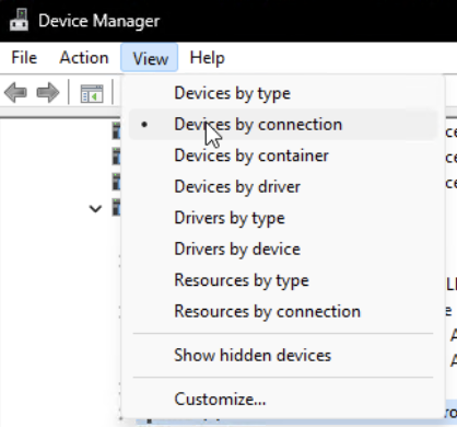
By selecting this view, we get to see the full topology of the system from the root PNP (Plug-N-Play) node. The PNP root node is the root of the tree of all devices on Windows, regardless of what bus or protocol they use. Every device, whether virtual or physical, is enumerated and placed onto this PNP tree. We can view the layout of this tree utilizing this view of the Device Manager.
In particular, we are looking to find the layout of the PCI devices on the system. That way, we can begin to build a visual model of what the PCI tree looks like on this machine. To do that, we need to locate the root of the PCI tree: the Root Complex. The Root Complex (abbreviated RC) is the owner of all things PCIe on the system. It is located physically on the CPU silicon and it is responsible for acting as the host that all PCIe devices receive and send packets with. It can be thought of as the bridge between software (the instructions executing on your machine) and hardware (the outside world of PCIe and RAM).
On this system, it is found in the PNP hierarchy here:
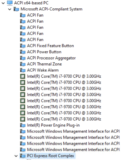
NOTE: You might be asking now “if PCI runs the show, why isn’t the PCI Root Complex at the top of the tree?” The answer to that is due to the fact that the PCIe bus is not the initial layout of the system presented by firmware during boot. Instead, ACPI (Advanced Configuration & Power Interface) is what describes the existence of PCIe to the OS. While you would never see it in a PC, it is possible to describe a system with no PCI bus and everything being presented purely by ACPI. We will talk more about ACPI later, but for now do not worry about this too much, just know that ACPI is how firmware tells us where the Root Complex is located, which then helps the OS enumerate PCI devices in the tree.
So now we know that the Root Complex is the top of the PCIe tree, now let’s take a look at what all is underneath it:
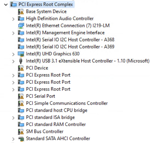
Unsurprisingly, there are many devices on this PCI bus. Here we can see all sorts of controllers responsible for Audio, Integrated Graphics, USB, Serial, and SATA. In addition, we see a few of these devices known as PCI Express Root Port. A Root Port is a port on the Root Complex where another PCIe Endpoint (aka a physical ‘device’) or Switch (aka a ‘router’) can be connected to. For PCI specification sake, you will hear Endpoints referred to as Type 0 devices, and Switch (or a Bridge) referred to as Type 1 devices, due to the fact that one is configured as a device to talk to and the other is configured as a device to route packets. An RC will have as many root ports as it physically supports. That is, as many as can be connected to the CPU silicon. Some root ports on a CPU might be routed directly to a physical PCIe slot, while others might be routed to other types of slots like an NVMe slot. It might also be routed to another PCIe switching device, which can route packets to multiple ports and therefore multiple Endpoints at once.
I will keep bringing this comparison back up, but I feel it is important– if you already understand Ethernet switches, you already understand PCIe switches. You can imagine that these root ports are like Ethernet ports on your desktop computer. You could connect these directly to another device (such as a camera) or you could connect these to a switch like your home router/modem, which will switch packets to expose more connections with further devices and machines to talk to. In this case, the ethernet cords are instead copper wire connecting one PCIe port to another PCIe port, thereby making it “point-to-point”.
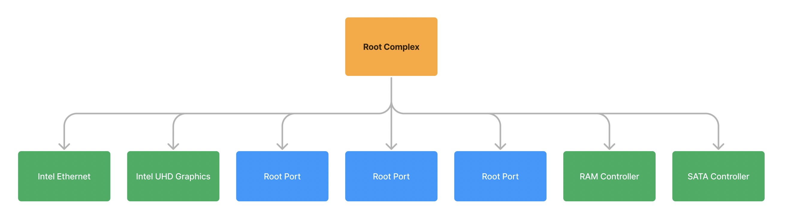
With this in mind, let’s start diagraming this hierarchy (partially) so we’re seeing it all laid out visually:
In PCI, all “busses” on the system are identified with a number from 0 to 255 (inclusive). In addition, all devices are identified with a “device id” and a “function id”. This is often seen described as Bus/Device/Function, or simply BDF. In more correct specification terms, this would be known as a RID (Requestor ID). To reduce confusion, I will refer to it as a BDF. BDF is important because it specifically tells us where in the PCIe hierarchy the device is located so we can communicate with it.
Because these are all on the top level of the hierarchy, we will give this “bus” a numerical identifier, it will be “Bus 0” or the Root Bus. We can verify that all of these devices are Bus 0 devices by right clicking a top level device and selecting Properties and looking at Location:
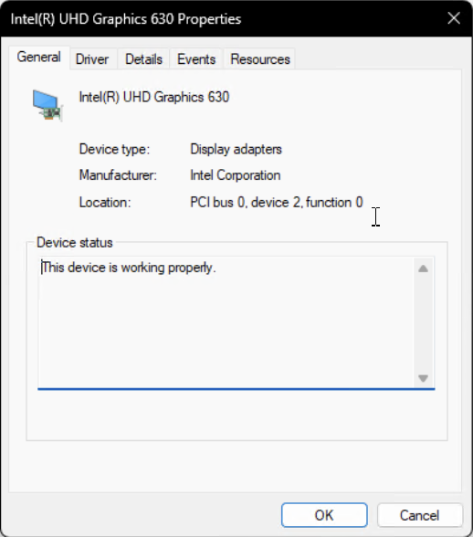
For this integrated graphics device, it is located with a BDF of 0:2.0. It is on Bus 0 (the Root Bus), a device id of 2, and a function id of 0. A “device” in this case represents a physical device, such as a graphics card. A “function” is a distinct capability that the physical device exposes to the system. It can, for all intents and purposes, be thought of as a separate entity. A device which exposes more than one function is aptly known as a Multi-Function Device (MFD). That means it exposes two or more PCI connections to the system while only physically being one device. We will look at an example of a real MFD soon.
An astute reader will notice that already we have already broken the “rule” I noted above: There are many devices connected to this singular Bus 0. This is the first exception to the “point-to-point” rule in PCIe and is only allowed in this case because Bus 0 is physically located on the silicon of the CPU. That is, there are no electrical traces between these devices, it is an imaginary connection. All of these devices exist inside the CPU package and routed using the extremely high speed electrical interconnects within it. These processor interconnects use an internal protocol that is specific to the vendor of the CPU and is not publicly documented, however we still communicate with it in the ‘language’ of PCIe. These endpoints (labelled in green), due to their special nature, will be given a special name: Root Complex Integrated Endpoints (RCIE), because they are integrated directly on the Root Complex.
This shouldn’t come as a surprise, you would expect that devices such as the integrated UHD graphics will be physically located on the CPU (as it is part of the specifications of the CPU). But we can learn about some more interesting topology of the system by observing other RCIEs, such as the fact that the RAM controller is also present here (the silicon which talks to the DRAM DIMMs of memory) and the USB controller (the silicon which talks to external USB devices). This is why certain CPUs only support certain kinds of RAM and USB specifications– because the devices which communicate are physically located on the CPU and only support the specification they were physically created to support.
UPDATE: This statement is incorrect. Some IO controllers can still be found on a discrete chip called the PCH (Intel) or also known as the chipset (AMD) which is nearby the CPU and has a high speed link that makes it seem like it is integrated into the CPU silicon. The above sentence incorrectly says that you can find the USB controller on the physical CPU, where it is more likely to be on the “chipset”. However, the memory controller that talks to RAM is found on the CPU die for speed purposes.
This diagram is a minimized version of the first level of the hierarchy, but now let’s build the rest of the hierarchy by expanding the rest of the Root Ports in the device manager.
And here’s what the filled in graph looks like:
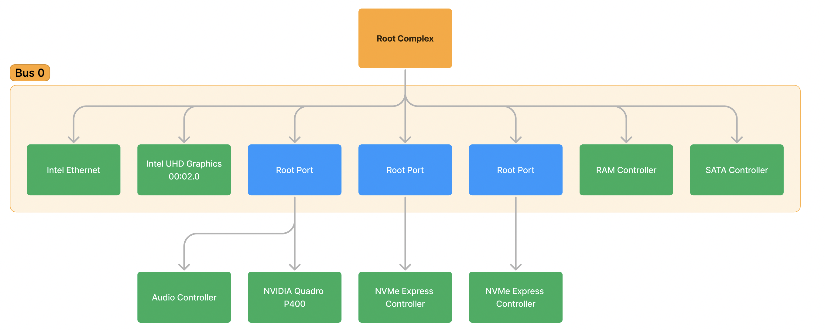
Note: I have marked the BDF of the UHD Graphics device and Bus 0.
These root ports are physically located on the CPU, but the devices attached to it are not. There are 3 devices connected to the external PCIe slots on this machine, a NVIDIA Quadro P400 graphics card and two NVMe drives. By going to the properties of each of these in Device Manager, we can pull and update their BDF information in the visual:
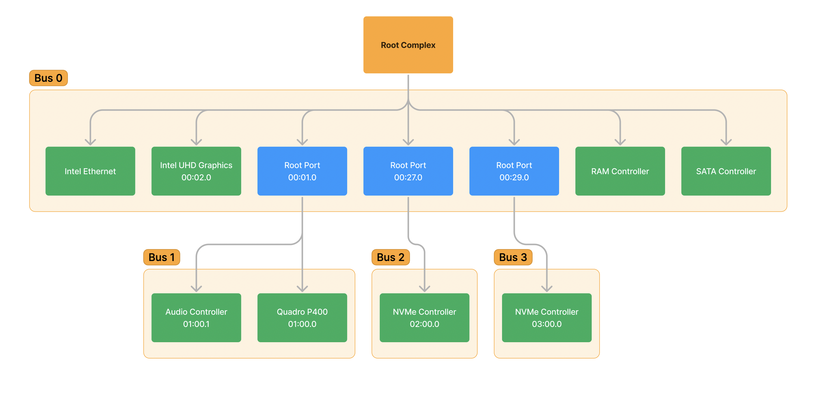
Underneath each of the root ports, we can see a device is physically connected. But, we can also see we have been exposed a new Bus under each. The Root Port has acted as a Bridge, it has bridged us from Bus 0 into a new bus, therefore the new bus must be assigned a new numerical ID and all of the devices/functions underneath that port will inherit that new bus number. This is the same logic utilized by the OS/Firmware during bus enumeration during boot: All bridges and switches expose a new bus which must be assigned a new bus ID number.
In this case, we can also see a good example of a Multi-Function Device. The Quadro P400 graphics card is acting as a MFD with two functions. The first function is 0 (BDF 01:00.0) and is the graphics card device itself. The second function is 1 (BDF 01:00.1) and it is the audio controller that allows audio to be played out of the ports such as HDMI. These two functions are distinct– they serve entirely different purposes and have separate drivers and configuration associated with them, but they are still implemented by the same physical device, which is device 0, and is located on the same bus, which is bus 1. This is consistent with the point-to-point rule of PCIe, only one physical device can be connected to a link, therefore only one physical device can exist on the bus (other than the exception, bus 0).
Exploring PCIe hierarchy and devices from WinDbg
So far we’ve seen a standard PCI bus hierarchy by using Device Manager’s “View by Connection” functionality. There is another more detailed way to investigate a PCIe hierarchy: using the trusty kernel debug extensions provided by WinDbg.
NOTE: It is assumed that you understand how to set up a kernel debugger on a machine to continue following along. You can also use LiveKD for most exercises. If you do not, please refer to the guide provided by Microsoft: Set up KDNET
I have connected to a new test machine different than the one used above. We will walk through the process of graphing the hierarchy of this machine using the output of the debugger. We will also learn how to investigate information about the device through its configuration memory.
Once dropped into a debugger, we will start by using the !pcitree command. This will dump a textual tree diagram of the PCI devices enumerated on the system.
8: kd> !pcitree
Bus 0x0 (FDO Ext ffffdc89b9f75920)
  (d=0,  f=0) 80866f00 devext 0xffffdc89b0759270 devstack 0xffffdc89b0759120 0600 Bridge/HOST to PCI
  (d=1,  f=0) 80866f02 devext 0xffffdc89ba0c74c0 devstack 0xffffdc89ba0c7370 0604 Bridge/PCI to PCI
  Bus 0x1 (FDO Ext ffffdc89ba0aa190)
    No devices have been enumerated on this bus.
  (d=2,  f=0) 80866f04 devext 0xffffdc89ba0c94c0 devstack 0xffffdc89ba0c9370 0604 Bridge/PCI to PCI
  Bus 0x2 (FDO Ext ffffdc89ba0a8190)
    (d=0,  f=0) 10de13bb devext 0xffffdc89ba04f270 devstack 0xffffdc89ba04f120 0300 Display Controller/VGA
    (d=0,  f=1) 10de0fbc devext 0xffffdc89ba051270 devstack 0xffffdc89ba051120 0403 Multimedia Device/Unknown Sub Class
  (d=3,  f=0) 80866f08 devext 0xffffdc89ba0cb4c0 devstack 0xffffdc89ba0cb370 0604 Bridge/PCI to PCI
  Bus 0x3 (FDO Ext ffffdc89ba08f190)
    No devices have been enumerated on this bus.
  (d=5,  f=0) 80866f28 devext 0xffffdc89ba0cd4c0 devstack 0xffffdc89ba0cd370 0880 Base System Device/'Other' base system device
  (d=5,  f=1) 80866f29 devext 0xffffdc89ba0cf4c0 devstack 0xffffdc89ba0cf370 0880 Base System Device/'Other' base system device
  (d=5,  f=2) 80866f2a devext 0xffffdc89ba0d14c0 devstack 0xffffdc89ba0d1370 0880 Base System Device/'Other' base system device
  (d=5,  f=4) 80866f2c devext 0xffffdc89ba0d34c0 devstack 0xffffdc89ba0d3370 0800 Base System Device/Interrupt Controller
  (d=11, f=0) 80868d7c devext 0xffffdc89ba0d84c0 devstack 0xffffdc89ba0d8370 ff00 (Explicitly) Undefined/Unknown Sub Class
  (d=11, f=4) 80868d62 devext 0xffffdc89ba0da4c0 devstack 0xffffdc89ba0da370 0106 Mass Storage Controller/Unknown Sub Class
  (d=14, f=0) 80868d31 devext 0xffffdc89ba0dc4c0 devstack 0xffffdc89ba0dc370 0c03 Serial Bus Controller/USB
  (d=16, f=0) 80868d3a devext 0xffffdc89ba0de4c0 devstack 0xffffdc89ba0de370 0780 Simple Serial Communications Controller/'Other'
  (d=16, f=3) 80868d3d devext 0xffffdc89ba0e04c0 devstack 0xffffdc89ba0e0370 0700 Simple Serial Communications Controller/Serial Port
  (d=19, f=0) 808615a0 devext 0xffffdc89ba0e24c0 devstack 0xffffdc89ba0e2370 0200 Network Controller/Ethernet
  (d=1a, f=0) 80868d2d devext 0xffffdc89ba0e44c0 devstack 0xffffdc89ba0e4370 0c03 Serial Bus Controller/USB
  (d=1b, f=0) 80868d20 devext 0xffffdc89ba0254c0 devstack 0xffffdc89ba025370 0403 Multimedia Device/Unknown Sub Class
  (d=1c, f=0) 80868d10 devext 0xffffdc89ba0274c0 devstack 0xffffdc89ba027370 0604 Bridge/PCI to PCI
  Bus 0x4 (FDO Ext ffffdc89ba0a9190)
    No devices have been enumerated on this bus.
  (d=1c, f=1) 80868d12 devext 0xffffdc89ba02c4c0 devstack 0xffffdc89ba02c370 0604 Bridge/PCI to PCI
  Bus 0x5 (FDO Ext ffffdc89b9fe6190)
    No devices have been enumerated on this bus.
  (d=1c, f=3) 80868d16 devext 0xffffdc89ba02e4c0 devstack 0xffffdc89ba02e370 0604 Bridge/PCI to PCI
  Bus 0x6 (FDO Ext ffffdc89ba0a7190)
    (d=0,  f=0) 12838893 devext 0xffffdc89ba062270 devstack 0xffffdc89ba062120 0604 Bridge/PCI to PCI
    Bus 0x7 (FDO Ext ffffdc89ba064250)
      No devices have been enumerated on this bus.
  (d=1c, f=4) 80868d18 devext 0xffffdc89ba0304c0 devstack 0xffffdc89ba030370 0604 Bridge/PCI to PCI
  Bus 0x8 (FDO Ext ffffdc89ba0b2190)
    No devices have been enumerated on this bus.
  (d=1d, f=0) 80868d26 devext 0xffffdc89ba0364c0 devstack 0xffffdc89ba036370 0c03 Serial Bus Controller/USB
  (d=1f, f=0) 80868d44 devext 0xffffdc89ba0384c0 devstack 0xffffdc89ba038370 0601 Bridge/PCI to ISA
  (d=1f, f=2) 80868d02 devext 0xffffdc89ba03a4c0 devstack 0xffffdc89ba03a370 0106 Mass Storage Controller/Unknown Sub Class
  (d=1f, f=3) 80868d22 devext 0xffffdc89ba03c4c0 devstack 0xffffdc89ba03c370 0c05 Serial Bus Controller/Unknown Sub Class
NOTE: If you have an error
Error retrieving address of PciFdoExtensionListHead, make sure your symbols are set up correctly and run.reload pci.systo reload PCI’s symbols.
When presented with this output, it might be difficult to visually see the “tree” due to the way the whitespace is formatted. The way to interpret this output is to look at the indentation of the Bus 0x text. Anything indented one set of spaces further than the Bus 0x line is a device on that bus. We can see there are also other Bus 0x lines directly underneath a device. That means that the device above the Bus 0x line is exposing a new bus to us, and the bus number is given there.
Let’s take look at a specific portion of this output:
Bus 0x0 (FDO Ext ffffdc89b9f75920)
  (d=0,  f=0) 80866f00 devext 0xffffdc89b0759270 devstack 0xffffdc89b0759120 0600 Bridge/HOST to PCI
  (d=1,  f=0) 80866f02 devext 0xffffdc89ba0c74c0 devstack 0xffffdc89ba0c7370 0604 Bridge/PCI to PCI
  Bus 0x1 (FDO Ext ffffdc89ba0aa190)
    No devices have been enumerated on this bus.
  (d=2,  f=0) 80866f04 devext 0xffffdc89ba0c94c0 devstack 0xffffdc89ba0c9370 0604 Bridge/PCI to PCI
  Bus 0x2 (FDO Ext ffffdc89ba0a8190)
    (d=0,  f=0) 10de13bb devext 0xffffdc89ba04f270 devstack 0xffffdc89ba04f120 0300 Display Controller/VGA
    (d=0,  f=1) 10de0fbc devext 0xffffdc89ba051270 devstack 0xffffdc89ba051120 0403 Multimedia Device/Unknown Sub Class
  (d=3,  f=0) 80866f08 devext 0xffffdc89ba0cb4c0 devstack 0xffffdc89ba0cb370 0604 Bridge/PCI to PCI
  Bus 0x3 (FDO Ext ffffdc89ba08f190)
    No devices have been enumerated on this bus.
In this output, we can see the BDF displayed of each device. We can also see a set of Root Ports that exist on Bus 0 that do not have any devices enumerated underneath, which means that the slots have not been connected to any devices.
It should be easier to see the tree structure here, but let’s graph it out anyways:
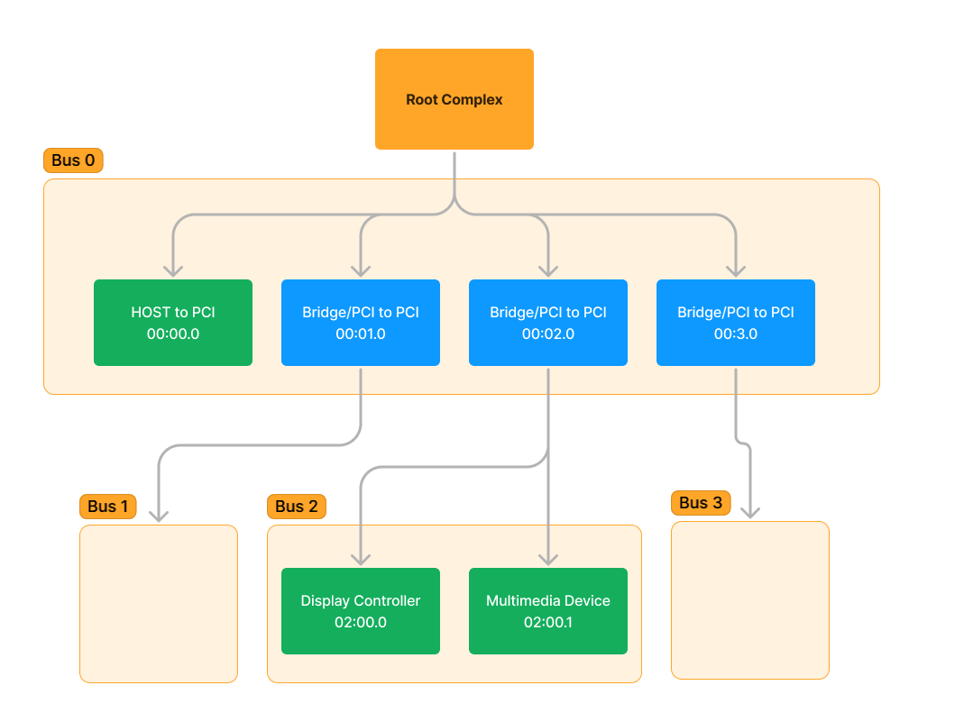
NOTE: It is just a coincidence that the bus numbers happen to match up with the device numbers of the Bridge/PCI to PCI ports.
As you now know, the devices labelled as Bridge/PCI to PCI are in fact Root Ports, and the device on Bus 2 is in fact a Multi-Function Device. Unlike the device manager, we don’t see the true name of the device from !pcitree. Instead, we are just given a generic PCI name for what “type” of the device advertises itself as. This is because Device Manager is reading the name of the device from the driver and not directly from PCI.
To see more about what this Display Controller device is, we can use the command !devext [pointer], where [pointer] is the value directly after the word devext in the layout. In this case, it is:
(d=0, f=0) 10de13bb devext 0xffffdc89ba04f270 devstack 0xffffdc89ba04f120 0300 Display Controller/VGA
!devext 0xffffdc89ba04f270
From here, we will get a printout of a summary of this PCI device as seen from the PCI bus driver in Windows, pci.sys:
8: kd> !devext 0xffffdc89ba04f270
PDO Extension, Bus 0x2, Device 0, Function 0.
  DevObj 0xffffdc89ba04f120  Parent FDO DevExt 0xffffdc89ba0a8190
  Device State = PciStarted
  Vendor ID 10de (NVIDIA CORPORATION)  Device ID 13BB
  Subsystem Vendor ID 103c (HEWLETT-PACKARD COMPANY)  Subsystem ID 1098
  Header Type 0, Class Base/Sub 03/00  (Display Controller/VGA)
  Programming Interface: 00, Revision: a2, IntPin: 01, RawLine 00
  Possible Decodes ((cmd & 7) = 7): BMI
  Capabilities: Ptr=60, power msi express
  Express capabilities: (BIOS controlled)
  Logical Device Power State: D0
  Device Wake Level:          Unspecified
  WaitWakeIrp:                <none>
  Requirements:     Alignment Length    Minimum          Maximum
    BAR0    Mem:    01000000  01000000  0000000000000000 00000000ffffffff
    BAR1    Mem:    10000000  10000000  0000000000000000 ffffffffffffffff
    BAR3    Mem:    02000000  02000000  0000000000000000 ffffffffffffffff
    BAR5     Io:    00000080  00000080  0000000000000000 00000000ffffffff
      ROM BAR:      00080000  00080000  0000000000000000 00000000ffffffff
    VF BAR0 Mem:    00080000  00080000  0000000000000000 00000000ffffffff
  Resources:        Start            Length
    BAR0    Mem:    00000000f2000000 01000000
    BAR1    Mem:    00000000e0000000 10000000
    BAR3    Mem:    00000000f0000000 02000000
    BAR5     Io:    0000000000001000 00000080
  Interrupt Requirement:
    Line Based - Min Vector = 0x0, Max Vector = 0xffffffff
    Message Based: Type - Msi, 0x1 messages requested
  Interrupt Resource:    Type - MSI, 0x1 Messages Granted
There is quite a lot of information here that the kernel knows about this device. This information was retrieved through Configuration Space (abbrev. “config space”), a section of memory on the system which allows the kernel to enumerate, query info, and setup PCI devices in a standardized way. The software reads memory from the device to query information such as the Vendor ID, and the device (if it is powered on) responds back with that information. In the next section, I will discuss more about how this actually takes place, but know that the information queried here was produced from config space.
So let’s break down the important stuff:
- DevObj: The pointer to the
nt!_DEVICE_OBJECTstructure which represents the physical device in the kernel. - Vendor ID: A 16-bit id number which is registered to a particular device manufacturer. This value is standardized, and new vendors must be assigned a unique ID by the PCI-SIG so they do not overlap. In this case, we see this is a NVIDIA graphics card.
- Device ID: A 16-bit id number for the particular chip doing PCIe. Similar idea in that a company must request a unique ID for their chip so it doesn’t conflict with any others.
- Subsystem Vendor ID: The vendor id of the board the chip sits on. In this case, “HP” is the producer of the graphics card, and “NVIDIA” designed the graphic chip.
- Subsystem Device ID: The device id of the board the chip sits on.
- Logical Device Power State: The power state of this device. There are two major power states in PCI, D0 = Device is powered on, D3 = Device is in a low-power state, or completely off.
- Requirements: The memory requirements the device is asking the OS to allocate for it. More on this later.
- Resources: The memory resources assigned to this device by the OS. This device is powered on and started already, so it already has its resources assigned.
- Interrupt Requirement/Resource: Same as above, except for interrupts.
To actually get the full information about this device, we can use the fantastic tool at PCI Lookup to query the public information about PCI devices registered with the PCI-SIG. Let’s put the information about the device and vendor ID into the box:

And when we search, we get back this:

Which tells us this device is a Quadro K620 graphics card created by NVIDIA. The subsystem ID tells us that this particular card PCB was produced by HP, which was licensed out by NVIDIA.
What we saw in !devext is a good overview of what pci.sys specifically cares about showing us in the summary, but it only scratches the surface of all of the information in config space. To dump all of the information in configuration space, we can use the extension !pci 100 B D F where BDF is the BDF of our device in question. 100 is a set of flags that specifies that we want to dump all information about the device. The information displayed will be laid out in the order that it exists in the config space of the device. Prefixing each section is an offset, such as 02 for device id. This specifies the offset into config space that this value was read from. These offsets are detailed in the PCI specification and do not change between PCI versions for backwards compatibility purposes.
8: kd> !pci 100 2 0 0

PCI Configuration Space (Segment:0000 Bus:02 Device:00 Function:00)
Common Header:
    00: VendorID       10de Nvidia Corporation
    02: DeviceID       13bb
    04: Command        0507 IOSpaceEn MemSpaceEn BusInitiate SERREn InterruptDis
    06: Status         0010 CapList
    08: RevisionID     a2
    09: ProgIF         00 VGA
    0a: SubClass       00 VGA Compatible Controller
    0b: BaseClass      03 Display Controller
    0c: CacheLineSize  0000
    0d: LatencyTimer   00
    0e: HeaderType     80
    0f: BIST           00
    10: BAR0           f2000000
    14: BAR1           e000000c
    18: BAR2           00000000
    1c: BAR3           f000000c
    20: BAR4           00000000
    24: BAR5           00001001
    28: CBCISPtr       00000000
    2c: SubSysVenID    103c
    2e: SubSysID       1098
    30: ROMBAR         00000000
    34: CapPtr         60
    3c: IntLine        00
    3d: IntPin         01
    3e: MinGnt         00
    3f: MaxLat         00
Device Private:
    40: 1098103c 00000000 00000000 00000000
    50: 00000000 00000001 0023d6ce 00000000
    60: 00036801 00000008 00817805 fee001f8
    70: 00000000 00000000 00120010 012c8de1
    80: 00003930 00453d02 11010140 00000000
    90: 00000000 00000000 00000000 00040013
    a0: 00000000 00000006 00000002 00000000
    b0: 00000000 01140009 00000000 00000000
    c0: 00000000 00000000 00000000 00000000
    d0: 00000000 00000000 00000000 00000000
    e0: 00000000 00000000 00000000 00000000
    f0: 00000000 00000000 00000000 00000000
Capabilities:
    60: CapID          01 PwrMgmt Capability
    61: NextPtr        68
    62: PwrMgmtCap     0003 Version=3
    64: PwrMgmtCtrl    0008 DataScale:0 DataSel:0 D0

    68: CapID          05 MSI Capability
    69: NextPtr        78
    6a: MsgCtrl        64BitCapable MSIEnable MultipleMsgEnable:0 (0x1) MultipleMsgCapable:0 (0x1)
    6c: MsgAddrLow     fee001f8
    70: MsgAddrHi      0
    74: MsgData        0

    78: CapID          10 PCI Express Capability
    79: NextPtr        00
    7a: Express Caps   0012 (ver. 2) Type:LegacyEP
    7c: Device Caps    012c8de1
    80: Device Control 3930 bcre/flr MRR:1K NS ap pf ET MP:256 RO ur fe nf ce
    82: Device Status  0000 tp ap ur fe nf ce
    84: Link Caps      00453d02
    88: Link Control   0140 es CC rl ld RCB:64 ASPM:None
    8a: Link Status    1101 SCC lt lte NLW:x16 LS:2.5
    9c: DeviceCaps2    00040013 CTR:3 CTDIS arifwd aor aoc32 aoc64 cas128 noro ltr TPH:0 OBFF:1 extfmt eetlp EETLPMax:0
    a0: DeviceControl2 0000 CTVal:0 ctdis arifwd aor aoeb idoreq idocom ltr OBFF:0 eetlp

Enhanced Capabilities:
    100: CapID         0002 Virtual Channel Capability
         Version       1
         NextPtr       258
    0104: Port VC Capability 1        00000000
    0108: Port VC Capability 2        00000000
    010c: Port VC Control             0000
    010e: Port VC Status              0000
    0110: VC Resource[0] Cap          00000000
    0114: VC Resource[0] Control      800000ff
    011a: VC Resource[0] Status       0000

    258: CapID         001e L1 PM SS Capability
         Version       1
         NextPtr       128
    25c: Capabilities  0028ff1f  PTPOV:5 PTPOS:0 PCMRT:255 L1PMS ASPML11 ASPML12 PCIPML11 PCIPML12
    260: Control1      00000000  LTRL12TS:0 LTRL12TV:0 CMRT:0 aspml11 aspml12 pcipml11 pcipml12
    264: Control2      00000028  TPOV:5 TPOS:0

    128: CapID         0004 Power Budgeting Capability
         Version       1
         NextPtr       600

    600: CapID         000b Vendor Specific Capability
         Version       1
         NextPtr       000
         Vendor Specific ID 0001 - Ver. 1  Length: 024
The nice thing about this view is that we can see detailed information about the Capabilities section of config space. Capabilities is a set of structures within the config space that describes exactly what features device is capable of. Capabilities includes information such as link speed and what kinds of interrupts the device supports. Any new features added to the PCI specification will be advertised through these structures, and the structures form a linked list of capabilities in config space that can be iterated through to discover all capabilities of the device. Not all of these capabilities are relevant to the OS, some are relevant only to aspects of hardware not covered by this post. For now, I won’t go into any further details of the capabilities of this device.
PCIe: It’s all about memory
So now that we’ve investigated a few devices and the hierarchy of a PCI bus, let’s talk about how the communication with software and PCI devices actually works. When I was first learning about PCI, I had a lot of trouble understanding what exactly was happening when software interfaces with a PCI device. Because the entire transaction is abstracted away from you as the software developer, it’s hard to build the mental model of what’s going on by just poking at PCI memory from a debugging tool. Hopefully this writeup will provide a better overview than what I was able to get when I was first starting out.
First off I will make a bold statement: All modern PCIe communication is done through memory reads and writes. If you understand how memory in PCIe works, you will understand how PCIe software communication works. (Yes, there are other legacy ways to communicate on certain platforms, but we will not discuss those because they are deprecated.)
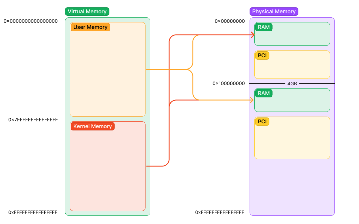
Now, let’s talk about different types of memory on a modern platform. The CPU of your OS after very early in boot will be using virtual memory. That is, the memory addresses seen by your CPU are the view of memory mapped to the physical memory world.
For our purposes, there are two types of physical memory on a system:
- RAM - Addresses that, when read or written to, is stored and retrieved from the DRAM DIMMs on your machine. This is what most people think of when they think “memory”.
- Device Memory - Addresses that, when read or written to, talks to a device on the system. The keyword here is talks. It does not store memory on the device, it does not retrieve memory on the device (although the device might be able to both). The address you might be talking to might not even be memory at all, but a more ethereal “device register” that configures the inner workings of the device. It is up to the device what happens with this kind of access. All you are doing is communicating with a device. You will typically see this referred to as MMIO, which stands for Memory-Mapped I/O.
NOTE: Device memory for PCI will always read “all 1s” or “all FFs” whenever a device does not respond to the address accessed in a device memory region. This is a handy way to know when a device is actually responding or not. If you see all FFs, you know you’re reading invalid device addresses.
It is a misunderstanding of beginners that all physical memory is RAM. When software talks to a PCI device in the PCI region, it is not reading and writing from RAM. The device instead is receiving a packet (a TLP, Transmission-Layer Packet) from the Root Complex that is automatically generated for you by your CPU immediately when the address inside the PCI region is read/written. You do not create these packets in software, and all of these packets are generated completely behind the scenes as soon as this memory is accessed. In software, you cannot even see or capture these packets, instead requiring a special hardware testing device to intercept and view the packets being sent. More on this later.
If it helps, think of physical memory instead as a mapping of devices. RAM is a device which is mapped into physical memory for you. PCI also has regions mapped automatically for you. Though they are distinct and act very differently, they look the same to software.
In the following diagram, we can see how a typical system is mapping virtual memory to physical memory. Note that there are two regions of RAM and two regions of PCI memory. This is because certain older PCI devices can only address 32-bits of memory. Therefore, some RAM is moved up above 4GB if your RAM does not fit within the window of addresses under 4GB. Since your processor supports 64-bit addresses, this is not an issue. Additionally, a second window is created above the 4GB line for PCI devices which do support 64-bit addresses. Because the 4GB region can be very constrained, it is best for devices to move as much memory above 4GB as to not clutter the space below.
Let’s talk first about the type of memory we’ve already seen: configuration space.
Configuration space is located in a section of memory called ECAM which stands for Extended Configuration Access Management. Because it is a form of device memory, in order to access this memory from the kernel (which uses virtual memory), the kernel must ask the memory manager to map this physical memory into a virtual address. Then, software instructions can use the virtual address of the mapping to read and write from physical addresses. On Windows, locating and mapping this memory is handled partially by pci.sys, partially by acpi.sys, and partially by the kernel (specifically the HAL).
NOTE: Typically the way device memory is mapped in Windows is through MmMapIoSpaceEx, which is an API drivers can use to map physical device memory. However, in order to do configuration space accesses, software must use HalGetBusDataByOffset and HalSetBusDataByOffset to ensure that the internal state of pci.sys is kept in synchronization with the configuration space reads/writes you are doing. If you try to map and change configuration space yourself, you might desync state from pci.sys and cause a BSOD.
NOTE: Where in physical memory the ECAM/PCI regions are located is platform dependent. The firmware at boot time will assign all special regions of physical memory of the system. The firmware then advertises the location of these regions to the OS during boot time. On x86-64 systems, the ECAM region will be communicated from firmware through ACPI using a table (a structure) called MCFG. Is it not important for now to know what specific protocol is used to retrieve this info, just understand that the OS retrieves the addresses of these regions from the firmware, which decided where to put them.
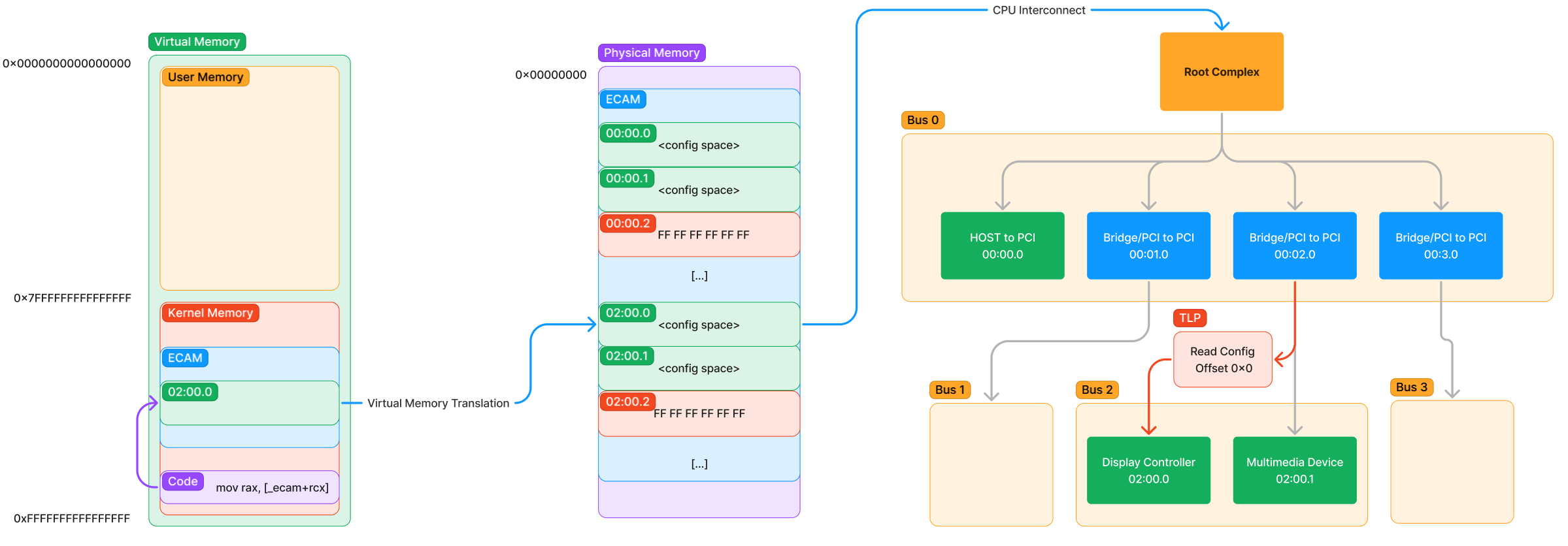
So in order to do a configuration space access, the kernel must map configuration space (ECAM) to virtual memory. This is what such a thing would look like:
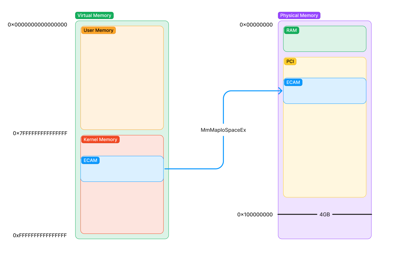
After this, the kernel is now able to communicate with the configuration space of the device by using the virtual mapping. But what does this configuration space look like? Well, it’s just a bunch of blocks of configuration space structures we talked about above. Each possible BDF a device could have is given space in ECAM to configure it. It is laid out in such a way that the BDF of the device tells you exactly where its configuration space is in ECAM. That is, given a BDF, we can calculate the offset to add to the base of the ECAM region in order to talk to the device because all ECAM regions for each function are the same size.
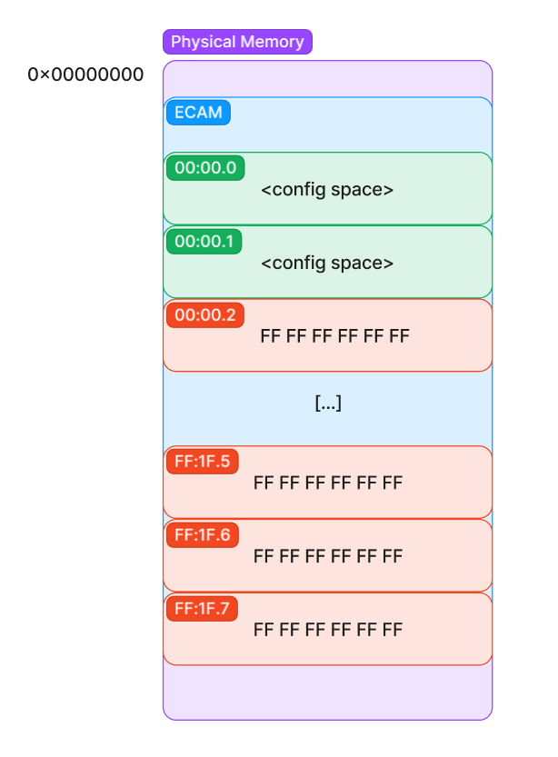
From this diagram, we can start to see how the enumeration of PCIe actually takes place. When we read back valid config space data, we know a device exists at that BDF. If we read back FFs instead, we know the device is not in that slot or function. Of course, we don’t brute force every address in order to enumerate all devices, as that would be costly due to the overhead of the MMIO. But, a smart version of this brute force is how we can quickly enumerate all devices powered up and responding to us on config space.
Putting it all together - A software config space access
Now that we see how config space is accessed, we can put the two sides together (the hierarchy and the MMIO) in to see the full path of an instruction reading config space from kernel mode.
Let’s step through the entire path taken here (from left to right):
- Some code running in kernel mode reads an offset from the ECAM virtual mapping.
- The virtual mapping is translated by the page tables of the CPU into a physical address into ECAM.
- The physical address is read, causing an operation to happen in the internal CPU Interconnect to inform the Root Complex of the access.
- The Root Complex generates a packetized version of the request as a TLP that says “Read the value at offset 0x0 for device 02:00.0” and sends it through the hierarchy.
- The TLP is received by this display controller on Bus 2 and sees that it is a configuration space TLP. It now knows to respond with a configuration space response TLP that contains the contents of the value at offset 0x0.
Now let’s look at the response:
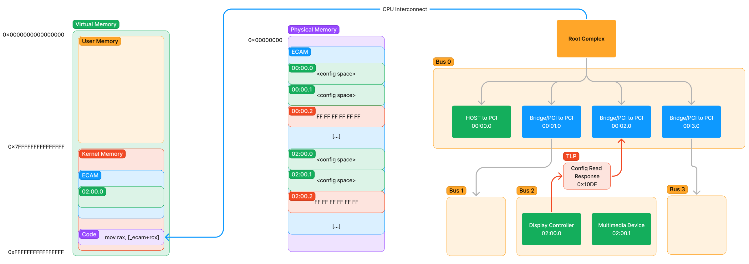
The path of the response is much less interesting. The device responds with a special TLP containing the value at offset 0 (which we know is the Vendor ID). That packet makes its way back to the Requester (which was the Root Complex) and the interconnect informs the CPU to update the value of rax to the value of 0x10DE which is the vendor ID of the NVIDIA graphics card. The next instruction then begins to execute on the CPU.
As you can imagine, accesses this way can be quite a lot slower than that of RAM with all of this TLP generation. This is indeed true, and one of the main reasons there is more ways than this MMIO method in order to talk to a device. In the next post, I will go into more detail about the other method, DMA, and its vital importance to the ensuring that software can transfer memory as fast as possible between the CPU and the device.
Exercise: Accessing ECAM manually through WinDbg
So, we took a look at how a config space access theoretically happens, but let’s do the same thing ourselves with a debugger. To do that, we will want to:
- Locate where ECAM is on the system.
- Calculate the offset into ECAM to read the Vendor ID of the the device. For this, I chose the
Multimedia Device@02:00.1which is on the NVIDIA graphics card. - Perform a physical memory read at that address to retrieve the value.
The first step is locate ECAM. This part is a little tricky given that the location of ECAM comes through ACPI, specifically the MCFG table in ACPI. This is the table firmware uses to tell the OS where ECAM is located in the physical memory map of the system. There is a lot to talk about with ACPI and how it is used in combination with PCI, but for now I’ll just quickly skip to the relevant parts to achieve our goal.
In our debugger, we can dump the cached copies of all ACPI tables by using !acpicache. To dump MCFG, click on the link MCFG to dump its contents, or type !acpitable MCFG manually:
8: kd> !acpicache
Dumping cached ACPI tables...
  XSDT @(fffff7b6c0004018) Rev: 0x1 Len: 0x0000bc TableID: SLIC-WKS
  MCFG @(fffff7b6c0005018) Rev: 0x1 Len: 0x00003c TableID: SLIC-WKS
  FACP @(fffff7b6c0007018) Rev: 0x4 Len: 0x0000f4 TableID: SLIC-WKS
  APIC @(fffff7b6c0008018) Rev: 0x2 Len: 0x000afc TableID: SLIC-WKS
  DMAR @(fffff7b6c000a018) Rev: 0x1 Len: 0x0000c0 TableID: SLIC-WKS
  HPET @(fffff7b6c015a018) Rev: 0x1 Len: 0x000038 TableID: SLIC-WKS
  TCPA @(ffffdc89b07209f8) Rev: 0x2 Len: 0x000064 TableID: EDK2
  SSDT @(ffffdc89b0720a88) Rev: 0x2 Len: 0x0003b3 TableID: Tpm2Tabl
  TPM2 @(ffffdc89b0720e68) Rev: 0x3 Len: 0x000034 TableID: EDK2
  SSDT @(ffffdc89b07fc018) Rev: 0x1 Len: 0x0013a1 TableID: Plat_Wmi
  UEFI @(ffffdc89b07fd3e8) Rev: 0x1 Len: 0x000042 TableID:
  BDAT @(ffffdc89b07fd458) Rev: 0x1 Len: 0x000030 TableID: SLIC-WKS
  MSDM @(ffffdc89b07fd4b8) Rev: 0x3 Len: 0x000055 TableID: SLIC-WKS
  SLIC @(ffffdc89b07fd538) Rev: 0x1 Len: 0x000176 TableID: SLIC-WKS
  WSMT @(ffffdc89b07fd6d8) Rev: 0x1 Len: 0x000028 TableID: SLIC-WKS
  WDDT @(ffffdc89b0721a68) Rev: 0x1 Len: 0x000040 TableID: SLIC-WKS
  SSDT @(ffffdc89b2580018) Rev: 0x2 Len: 0x086372 TableID: SSDT  PM
  NITR @(ffffdc89b26063b8) Rev: 0x2 Len: 0x000071 TableID: SLIC-WKS
  ASF! @(ffffdc89b2606548) Rev: 0x20 Len: 0x000074 TableID:  HCG
  BGRT @(ffffdc89b26065e8) Rev: 0x1 Len: 0x000038 TableID: TIANO
  DSDT @(ffffdc89b0e94018) Rev: 0x2 Len: 0x021c89 TableID: SLIC-WKS
8: kd> !acpitable MCFG
HEADER - fffff7b6c0005018
  Signature:               MCFG
  Length:                  0x0000003c
  Revision:                0x01
  Checksum:                0x3c
  OEMID:                   HPQOEM
  OEMTableID:              SLIC-WKS
  OEMRevision:             0x00000001
  CreatorID:               INTL
  CreatorRev:              0x20091013
BODY - fffff7b6c000503c
fffff7b6`c000503c  00 00 00 00 00 00 00 00-00 00 00 d0 00 00 00 00  ................
fffff7b6`c000504c  00 00 00 ff 00 00 00 00                          ........
To understand how to read this table, unfortunately we need to look at the ACPI specification. Instead of making you do that, I will save you the pain and pull the relevant section here:
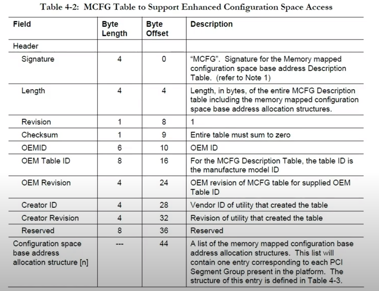
As the !acpitable command has already parsed and displayed everything up to Creator Revision in this table, the first 8 bytes of the BODY are going to be the 8 bytes of Reserved memory at offset 36. So, we skip those 8 bytes and find the following structure:
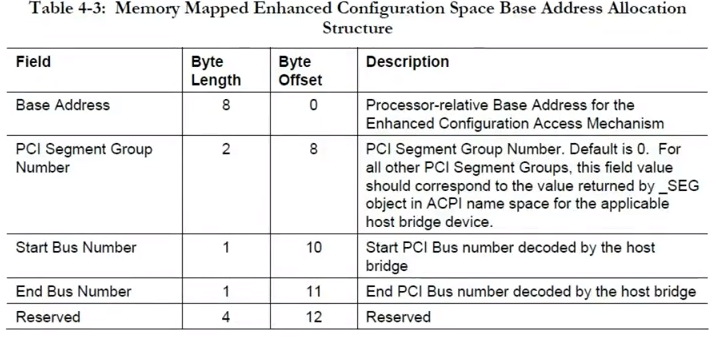
The first 8 bytes of this is the address of the ECAM region for the region following Reserved. So that means the offset of the ECAM base address is at offset 8.
BODY - fffff7b6c000503c
fffff7b6`c000503c  00 00 00 00 00 00 00 00-00 00 00 d0 00 00 00 00  ................
fffff7b6`c000504c  00 00 00 ff 00 00 00 00                          ........
For this system, ECAM is located at address: 0xD0000000. (Don’t forget to read this in little endian order)
To verify we got the correct address, let’s read the vendor ID of 00:00.0 which is also is the first 2 bytes of ECAM. We will do this using the !dw command, which stands for dump physical word (the exclamation point means physical). This command requires you specify a caching type, which for our case will always be [uc] for uncached. It also supplies a length, which is the number of words to read specified by L1.
NOTE: It is important that we always match the size of the target device memory to the size we are reading from software. This means, if the value we want to read is a 16-bit value (like Vendor ID), then we must perform a 16-bit read. Performing a 32-bit read might change the result of what the device responds with. For configuration space, we are okay to read larger sizes for Vendor ID, but this is not true in all cases. It’s good to get in the habit of matching the read size to the target size to avoid any unexpected results. Remember: Device memory is not RAM.
Putting that all together, we read the VendorID of 00:00.0 like so:
8: kd> !dw [uc] D0000000 L1
#d0000000 8086
The resulting value we read is 0x8086, which happens to be the vendor ID of Intel. To verify this is correct, let’s dump the same thing using !pci.
8: kd> !pci 100 0 0 0

PCI Configuration Space (Segment:0000 Bus:00 Device:00 Function:00)
Common Header:
    00: VendorID       8086 Intel Corporation
Reading VendorID from a specific Function
Now to calculate the ECAM address for another function we wish to talk to (NVIDIA card at 02:00.1), we will need to perform an “array access” manually by calculating the offset into ECAM using the BDF of the target function and some bit math.
The way to calculate this is present in the PCIe specification, which assigns a certain number of bits of ECAM for bus, device, and function to calculate the offset:
| 27 - 20 | 19 - 15 | 14 - 12     |  11 - 0       |
| Bus Nr  | Dev Nr  | Function Nr | Register      |
By filling in the BDF and shifting and ORing the results based on the bit position of each element, we can calculate an offset to add to ECAM.
I will use python but you can use whatever calculator you’d like:
>>> hex(0xD0000000 + ((2 << 20) | (0 << 15) | (1 << 12)))
'0xd0201000'
This means that the ECAM region for 02:00.1 is located at 0xD0201000.
Now to read the value of the VendorID from the function:
8: kd> !dw [uc] D0201000 L1
#d0201000 10de
The result was 0x10de, which we know from above is NVIDIA Corporation! That means we successfully read the first value from ECAM for this function.
Conclusion
This single post ended up being a lot longer than I expected! Rather than continue this single post, I will instead split this up and flesh out the series over time. There are so many topics I would like to cover about PCIe and only so much free time, but in the next post I will go into more detail about device BARs (a form of device-specific MMIO) and DMA (Direct Memory Access). This series will continue using the same tenants as before, focusing more on understanding rather than specific details.
Hopefully you enjoyed this small look into the world of PCIe! Be back soon with more.